- Subscribe to RSS Feed
- Mark Topic as New
- Mark Topic as Read
- Float this Topic for Current User
- Bookmark
- Subscribe
- Mute
- Printer Friendly Page
LabVIEW FPGA Desktop Execution Node Testbench Design
05-29-2019 01:39 PM
- Mark as New
- Bookmark
- Subscribe
- Mute
- Subscribe to RSS Feed
- Permalink
- Report to a Moderator
Hello folks,
I'd like some recommendations on how to handle creating an LVFPGA VI that can act as its own simulation source. The DEN requires a timing loop (while or SCTL) in the target VI, but my subVIs don't contain loops - only my top level. Is there a convenient way to incorporate loops such that my DEN works, but without having multiple copies of my controls and indicators so I don't have to rewire the connector pane when switching from TB to synthesis?
I am using LabVIEW 2017 with FPGA module. The Desktop Execution Node (DEN) allows the user to simulate the behavior of LabVIEW FPGA modules, and plot various boolean and numeric signals on a waveform. The DEN expects to point to a VI containing either a While Loop + Timing structures, or a Single Cycle Timed Loop. It then allows you to apply a top level "clock" as a stimulus source, as well as select Inputs to apply stimulus.
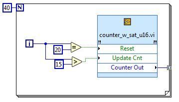
Example VI: U16 counter that saturates @ xFFFF rather than rollover.
As you can see, this subVI is meant to be instantiated in a while loop with looptimer, or SCTL.
Testbench: Do not increment for the first 15 clocks. Then increment for 5 clocks. Then reset the count. Then resume incrementing. End the simulation after 40 clocks elapsed.
Here are the issues I see:
- Since the subVI has no loop in it (counter subVI doesn't require that, when caller has a loop), the testbench won't run.
- If you add a loop to the subVI:
- Now there's an SCTL in an SCTL. I believe this probably synthesizes just fine, but I don't like that coding style (should I just get over this?)
- If I were to use a conditional disable to differentiate between synthesis and simulation, that will force me to duplicate controls/indicators and re-wire the connection pane. This is obviously a pain, because it won't switch automatically when I change the execution mode between FPGA and Simulation
- If I create a wrapper containing the SubVI in a SCTL, and target this wrapper with the DEN, then the sampling probes in the subVI will not report any signal values! This is obviously of no value to me.
So it really looks like my only two options are:
- Create multiple files (configuration mgmt nightmare)
- Make each subVI with a SCTL in it [call it "dut_counter"].
- Make a testbench with the test vectors and DEN ["tb_counter"].
- Once the dut has passed all of its tests, copy the contents of the SCTL into a new file called "counter". Any changes to the SubVI due to requirements changes later on would be first implemented in DUT and
- Leave an SCTL in each SubVI (is this acecptable)? I don't tend to use ANY while loops in my FPGAs, so I'm not worried about strange behaviors that might result from nested while loops.
Can you help provide some other suggestions for me to try, or other feedback?
05-29-2019 02:23 PM
- Mark as New
- Bookmark
- Subscribe
- Mute
- Subscribe to RSS Feed
- Permalink
- Report to a Moderator
EDIT: I just realized that nesting SCTLs is a no-no. I thought perhaps it would recognize and flatten the nests. It does not. Therefore, I don't have any streamlined way to procedurally switch between synthesizable and simulator-compatible subVIs.
Bummer.
05-29-2019 03:48 PM
- Mark as New
- Bookmark
- Subscribe
- Mute
- Subscribe to RSS Feed
- Permalink
- Report to a Moderator
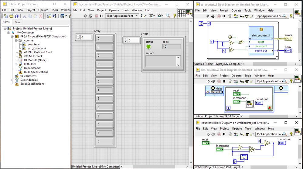
Yeah, nested SCTLs are not allowed, which definitely doesn't help you. The real issue that you're running into is that the DEN isn't really designed for "unit" testing like this. It's more for higher level "component" testing. That said, you can get the behavior you're looking for by adding in a wrapper VI on the FPGA side (that is really just for this simulation). A project organization would look something like this:
having the additional files in the project is definitely not ideal, but there isn't really a way around it... at least in LabVIEW 20XX.
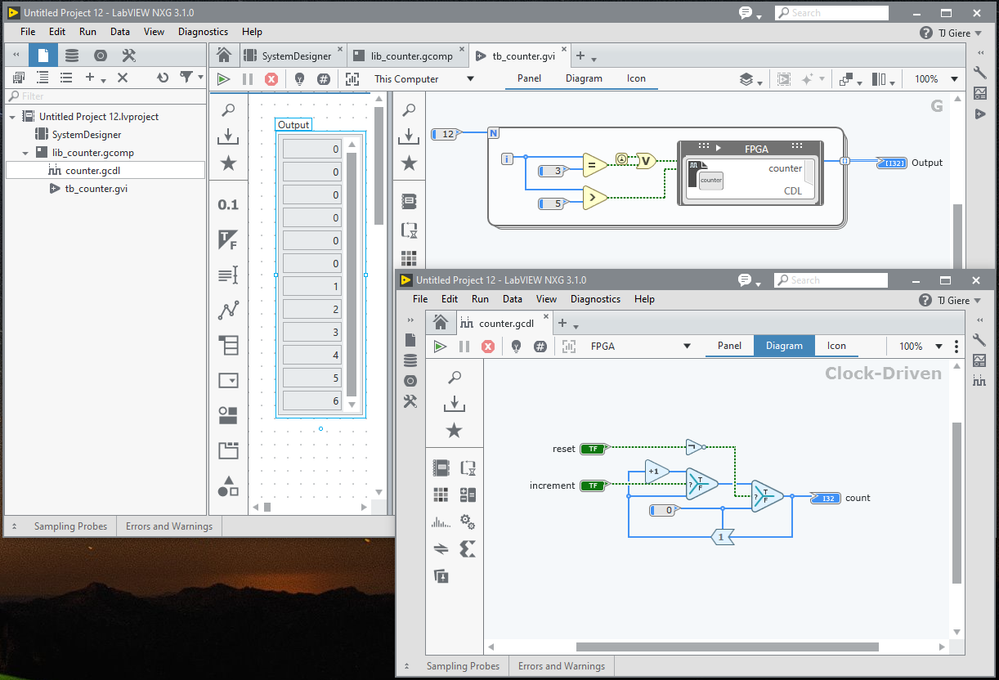
It doesn't really help your current project, but we actually went the other direction with LabVIEW NXG, and the node similar to the DEN behaves as you would have expected.
TJ G
05-29-2019
04:58 PM
- last edited on
01-21-2025
11:09 AM
by
![]() Content Cleaner
Content Cleaner
- Mark as New
- Bookmark
- Subscribe
- Mute
- Subscribe to RSS Feed
- Permalink
- Report to a Moderator
TJ - good to hear from you. As you know, I'm trying to develop a methodology for unit-testing my VI's. I've been becoming more proficient at the DEN and its intricacies. I've also been working through the Simulated I/O from VI functionality. Specifically, trying out this tutorial: https://www.ni.com/docs/en-US/bundle/labview-fpga-module/page/tutorial-creating-test-benches-fpga-mo...
I don't think that's really the greatest method either - it's wildly unreadable, and fairly obscure if you don't already know how to do it. I want to get out of the habit of manual checking of testbenches, but also would like the flexibility to probe deeper into subVIs if possible.
What does the NI staff use for Unit Test and/or regression testing of FPGA VI?
05-30-2019 08:33 AM
- Mark as New
- Bookmark
- Subscribe
- Mute
- Subscribe to RSS Feed
- Permalink
- Report to a Moderator
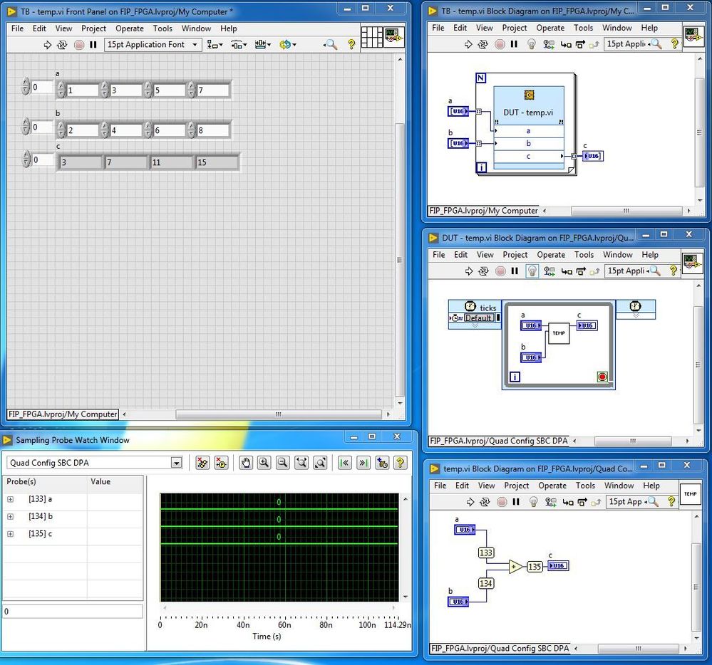
Also it's worth mentioning that your first example photo doesn't work in LV2017 for sampling probes.
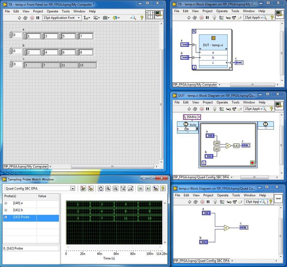
Specifically, the DEN will only allow probing of the VI that it points to. So having a SCTL wrapper around a SubVI block defeats the purpose of probing. Here's an adder example that illustrates that your example with the 'sim' wrapper doesn't work except as a black-box. This would work for "Verification" against a software model, and for use in a self-checking testbench. Doesn't really work for debugging.
Any visibility for debugging would need to be done with more copying and pasting. IE: the a DUT would need to be debugged, and then copied/pasted into its own non-SCTL VI, as shown here.
06-03-2019
05:00 PM
- last edited on
01-21-2025
11:10 AM
by
![]() Content Cleaner
Content Cleaner
- Mark as New
- Bookmark
- Subscribe
- Mute
- Subscribe to RSS Feed
- Permalink
- Report to a Moderator
Hi JJMontante,
I think you were already hinting at this in your first post but part of the problem here is that only certain block diagram nodes and structures will advance simulated time (i.e. While Loops and SCTLs) when using DEN. You can see a full list of those nodes here:
Using the LabVIEW FPGA Desktop Execution Node
In addition, I think that your definition of Unit Testing might be slightly different than the way it is defined for LabVIEW 20XX FPGA in our documentation. We recommend that Unit Testing in LabVIEW 20XX FPGA be executed by running code on the Windows PC. The Desktop Execution Node is considered "FPGA Simulation", even though the node itself is being called from the Windows PC. Here is the way Unit Testing is defined in our documentation:
"Execution of a VI in the Windows context is primarily used for unit testing and logic validation. Because a unit does not contain any FPGA-specific I/O or resources, you can execute the VI in the Windows context. To execute an FPGA VI in the Windows context, click and drag the VI from the FPGA target to My Computer in the LabVIEW project.
When you execute an FPGA VI in the Windows context, you can only verify the functionality of the VI. In the Windows context, none of the FPGA timing characteristics of the VI is preserved. To verify timing, you must integrate the unit into a component and test the unit in one of the other execution modes."
Taking this into account I think your unit testing would be running these VIs on the Windows PC to verify the functionality of the unit without DEN and without any timing. When the VI is running on the Windows PC you can use all of your standard LabVIEW debugging tools (breakpoints, highlight execution, probes, etc.). If some of the VIs that you want to unit test can't run on the Windows PC because of FPGA specific nodes or resources then it could be an indication that it needs to be broken down more to be tested at the unit level (as we've defined it). If you need to incorporate timing then it would no longer be unit testing.
My understanding of the intent of DEN is for it to be used at a higher level testing (i.e. component and above).
This tutorial contains the definitions and more detail on the various forms of testing:
Testing and Debugging LabVIEW FPGA Code
Finally, regarding organizing and maintaining separate code for simulation and hardware one thing that might be helpful is using a Conditional Disable Structure with the FPGA_EXECUTION_MODE symbol:
Configuring Conditions for Conditional Disable Structures
There is a simple LabVIEW example for this structure at:
Help>>Find Examples>>Fundamentals>>Loops and Structures>>Conditional Disable Structure.vi
All of that being said I think that you definitely have some valid concerns here. My intent with the above is to describe what I understand the purpose of DEN to be and what we've defined as unit testing.
Regards,
Kyle S.
06-04-2019 07:42 AM
- Mark as New
- Bookmark
- Subscribe
- Mute
- Subscribe to RSS Feed
- Permalink
- Report to a Moderator
Kyle -
Long post ahead, most of it is me trying to put my thoughts into writing. I'd like to achieve specific goals, with specific questions all the way at the end. I'd appreciate your input on those questions, and of course, let me know where my assumptions are wrong in what I've written below.
My goal is to try and create an ASIC/FPGA style verification flow with the following goals:
- SubVIs that are synthesizable are also testable (no SCTLs nested in them, no extra "helper VIs" to instantiate)
- VIs contain information on timing (I don't want to double verification time by verifying algorithm, then switching simulators and verifying timing if possible).
- Test SW developers don't need to know VHDL to write testbenches
- Used to be do-able with ModelSim + Simulation palette now deprecated in 2018.
- Not do-able with Xilinx Sim, because I don't have sim-palette calls when 3rd party sim is set to iSim.
- Minimize the LabVIEW FPGA specific knowledge that LV developers need to know to do verification
- Allow for scoreboarding / coverage
My current design flow basically forces me into a couple of directions I don't want:
- Using separate simulators for Socket CLIP and LVFPGA diagrams.
- Can do with iSim export, if testbench is coded in VHDL, in conflict with my desirement above.
- Used for creating off-chip models of stimulus generators tied to aUserGpio[n]
- Using multiple files for the DUT if using Desktop Execution Node
- Undesirable for Configuration management
- High probability of copy/paste errors between DUT and Synthesizable code
- Cannot use LV Simulation testbenches with iSim simulator, only modelsim
- Limits the project staff I can use, because I have no other team members that know VHDL
So to recap the advice given in this thread for a single VI with no hierarchy.
- Design a VI that performs a function in LVFPGA context.
- Design a VI testbench, stimulus generator, and checker that tests the DUT function in the Host computer context.
- Debug logic in this host-computer context.
- Design a wrapper VI containing timing (while loop + timers, or SCTL)
- Generate a 3rd Party Simulator wrapper, stimulus generator, checker.
- ModelSim/iSim : VHDL stimulus generator, and checker, paste and wire those into the TB_niFpga...Model.vhd
- Run VHDL tests and inspect for timing.
- Feed any debug information back into the original LabVIEW FPGA block diagram.
Which *ideally* requires the following resources:
1. LabVIEW FPGA source code
2. LabVIEW FPGA wrapper for timing
3. Labview Host code for stimulus generation, checking, and execution
4. 3rd-party simulation export
5. VHDL files for stimulus generator, checker
6. LabVIEW FPGA DUT programmer
7. LabVIEW Host testbench programmer (bad practice to trust testing to the author of the code)
8. VHDL testbench programmer (again, bad practice to let the author test their own code).
So here are my specific questions:
- Do you use a verification methodology similar to that just described above when new FPGA VIs are developed (for instance, R-Series VIs, FlexRIO VIs, express VIs like filters or RMS measurements)?
- Can you summarize at a high level, the verification process that NI uses, or describe how NI deviates from the process described above?
- Do you use the DEN ever for developing? When is it appropriate vs 3rd Party Sims?
- Do you ever use Simulated I/O from VIs for developing? When is it appropriate vs DEN or 3rd Party Sim?
- It appears to be most useful in cases where FPGA IO is used at the top-level rather than controls/indicators.
- Is there an official instructor-lead training that covers these topics in depth?
- Is there any tutorial or white paper which would show improvements to this process in NXG that would make a compelling argument for adoption of NXG for my next project?
- Are there specific tips/tricks documented for getting stimulus into a LVFPGA model? Examples I have found useful:
- Generate large test vectors in LV Host, use DMA FIFO to send to FPGA for simulation only. Use conditional disable to switch LVFPGA inputs from FPGA IO to DMA FIFO in simulation modes.
- Use conditional disable to change FPGA IO to controls/indicators for simulation modes for use on DEN or Simulated IO w/ VI.
Thanks!
Jim

