ni.com is currently undergoing scheduled maintenance.
Some services may be unavailable at this time. Please contact us for help or try again later.
- Subscribe to RSS Feed
- Mark Topic as New
- Mark Topic as Read
- Float this Topic for Current User
- Bookmark
- Subscribe
- Mute
- Printer Friendly Page
NI SPI IP or SPI Digital Waveform Library for the 16 bit SPI communication between NI sbRIO9607 and ADS1118 ADC in LabView
Solved!07-26-2017 03:51 AM - edited 07-26-2017 04:17 AM
- Mark as New
- Bookmark
- Subscribe
- Mute
- Subscribe to RSS Feed
- Permalink
- Report to a Moderator
Hi all,
I have found 2 libraries but could not understand what is the difference between them. I am trying to communicate with a ADC converter (ADS1118) by using SPI communication. It uses Mode1 (CPHA 1). I want to use 4 of sbRIO DIO pins to fully communicate (full duplex is preferred but half duplex is also acceptable for basic understanding). I have just 1 slave for now. But did not connected CS pin to GND, since I will need some specific CS configuration behavior for ADS1118.
I have worked many times with SPI protocol, microprocessors, ADC-DAC and FPGA's before, but not much with LabView. But this is the very first time I am trying to control NI sbRIO DIOs with LabView. I could understand the basic concepts. But sometimes something is missing, and I could not find a totaly detailed documentation for these libraries.

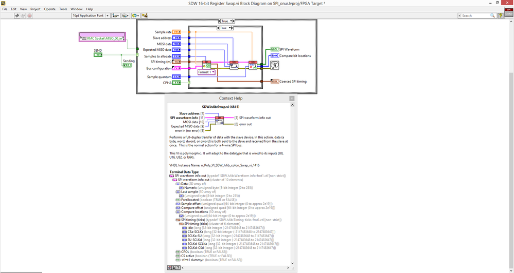
There is example VIs. In the example for the SPI Digital Waveform library, "swap" is used in this example, which I understand as it establishes a full duplex communication. But I could not assigned any DIO pin to it. Connecting wires from FPGA IO to "swap" are all broken all the time.
Is "Expected MISO data" meaning the coming ADS1118 MISO line? Is it the actual RAW MISO data line or is it just a simulation for MISO line in this VI? Am I able to use this pin directly by connecting a DIO pin to it? (I ask because it looks like it was just a referance line). If so, is there any way to receive any data from ADS1118 to my master device sbRIO?
In NI SPI IP; Spi Master.vi has a "spi input" and a "data to write" inputs which is U64. I think that "data to write" input is my MOSI line, but what then the "spi input" for? And for the output, "read data" output is given, but again U64. I have confused, because if this line is the MISO line, then does not it need to be boolean? I could not understand exactly the behaviour of the "manual chip assert", "start strobe" or "MOSI output enable done". They seems to me as they are not necesaary for SPI communication. How should they be used?
When I am trying to connect FPGA RMC DIO pins to any not boolean pin, the wire is broken since the type mismatch. How can I fix it? Choosing DIO pins U8 or U16 etc. did not work, because of the actual usage of the DIO PIN is just a bit, bit0.
Related Libraries are all in VIPM and example finder, sample swap.vi is attasched to this post also.
Thank you !!
Solved! Go to Solution.
07-27-2017
10:56 AM
- last edited on
04-15-2025
02:20 PM
by
![]() Content Cleaner
Content Cleaner
- Mark as New
- Bookmark
- Subscribe
- Mute
- Subscribe to RSS Feed
- Permalink
- Report to a Moderator
Hi Onrep,
Firstly, I thought I'd link you to the product page for that addon for some context.
SPI Digital Waveform Reference Library
The main thing is that you probably won't be able to use the reference libbrary because
it's meant for our HSDIO and hardware timed DAQ devices.
Those VIs won't run on FPGA and doing it on the host will result in it not being hardware timed.
In order to Implement SPI on RIO you usually need to create your own implementation on the FGPA.
However, there is a free add-on that has FPGA and host code to do this if they want
SPI and I2C Driver API - National Instruments
Another helpful document is one below:
Implementing SPI Communication Protocol in LabVIEW FPGA
Hopefully this is helpful in your application. Let me know if you have other specific Questions.
David Raji
08-07-2017 10:19 AM
- Mark as New
- Bookmark
- Subscribe
- Mute
- Subscribe to RSS Feed
- Permalink
- Report to a Moderator
First of all, thank you davidraj for your response,
For sbRIO 9607, it seems like I still have some problems with those libraries. Because of this, I decided to implement my very own SPI protocol in low level. I still have some problems, but now I could understand better what the problems are.
If I had further questions, I will again mention to this or a new post on NI forum.
Best regards
