- Document History
- Subscribe to RSS Feed
- Mark as New
- Mark as Read
- Bookmark
- Subscribe
- Printer Friendly Page
- Report to a Moderator
- Subscribe to RSS Feed
- Mark as New
- Mark as Read
- Bookmark
- Subscribe
- Printer Friendly Page
- Report to a Moderator
Light Intensity Measurement
Overview:
This document discusses basic light detection theory and applications, and explains how to use the myDAQ or ELVIS II series to obtain light intensity (specifically IR light) measurements. The light data will be acquired using the DAQ Assistant that is installed into LabVIEW with the NI DAQmx driver.
Purpose:
Use the myDAQ or ELVIS II to power an IR LED and measure its intensity with a phototransistor on a protoboard. The signal will be captured and displayed through LabVIEW.
Background:
Photodetectors sense and respond to light, and use several different modes of operation. A few of these modes are shown below:
- Photovoltaic cell (solar cell) -- produce a voltage and supply current when illuminated by exciting electrons into a higher state that allows them to act as charge carriers.
- Photoconductive – vary resistance based on illumination.
- Photoemissive – contain a photocathode that emits light when illuminated.
- Photoelectromagnetic – produce a voltage and supply current when illuminated through an intermetallic semiconductor in a magnetic field.
- Photoconductive – become more electrically conductive when illuminated.
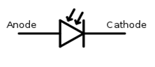
Figure 1: Photodiode Symbol
Photodiodes operate in either photoconductive or photovoltaic mode. In photoconductive mode, the diode is frequently reverse biased, meaning the cathode is positive. This mode reduces the response time but increases noise, and has a linear current response to illuminance. In photovoltaic mode, current out of the device is restricted and voltage builds up. Another form of a photodiode is a phototransistor, which is essentially a photodiode with internal gain. Phototransistors have higher responsivity than photodiodes, but do not detect low levels of light better than photodiodes.
In a photoconductive/photovoltaic detector, the p-n junction resistance and junction photocurrent change in response to the incident light. Reverse-biased diodes and transistors are typical elements for this category of photodetectors. They can operate in both the photoconductive and photovoltaic modes. The difference between the two constructions is defined primarily by semiconductor structures, which are introduced by p-n junction photodiodes, p-i-n (/ = intrinsic) photodiodes, avalanche photodiodes, photofets, pnp or npn junction transistors, and photodarlingtons.
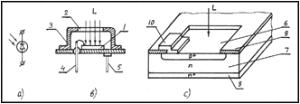
Figure 2: Photodiode Anatomy
Labels: a = photodiode symbol, b = photodiode package, c = photodiode structure; L = light flux, 1 = photodiode chip, 2 = transparent window, 3 = case, 4 and 5 = leads, 6 = photodiode anode, 7 = n-type substrate, 8 = n+ -diffused layer, 9 = silicon dioxide, 10 = metallization for anode contact.
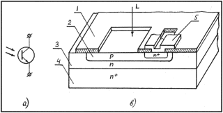
Figure 3: Phototransistor Anatomy
Labels: a = phototransistor symbol, b = phototransistor structure; L = light flux, 1 = silicon dioxide, 2 = p-type diffused layer, 3 = n-type epitaxial layer, 4 = n+ substrate, 5 = emitter contact.
One other thing to keep in mind is that all photodetectors respond differently to light with different wavelengths. The frequency response of the photodetector being used can be seen on its datasheet.
Light Measurement Applications
Light intensity measurements have a variety of applications. Cameras typically use charge coupled devices (CCD) or CMOS sensors to capture light intensities at very small points in space, which combine together to form an image. IR light intensity measurements is used by many proximity sensors, spectrometers, and other types of sensors. Free space optical communication is used by many different types of remote control systems, and all of them operate on the basic premise of transmitting and receiving an IR light signal.
Equipment:
- NI myDAQ or NI ELVIS II series
- LabVIEW
- Wire
- Breadboard
- Resistors: 220 Ω and 470 Ω
- Phototransistor
General Measurement:
A photodiode has both an anode and a cathode. It has a low forward resistance (anode positive) and high reverse resistance (anode negative). Most photodiodes operate by negative biasing the anode or positive biasing the cathode. In the photovoltaic and zero bias modes, the generated current or voltage is in the diode forward direction. Hence the generated polarity is opposite to that required for the biased mode. Based on the type of photodetector you are using, different configurations of measuring light intensity exist. The following are two of the most common configurations at a basic level:
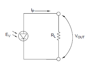
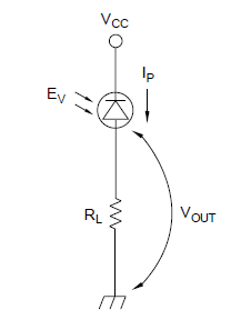
Figure 4: Fundamental Photodetector Circuit with Bias (left) and without Bias (right)
*Note that phototransistors can be substituted into the above circuits.
In addition to these topologies, photocurrent-voltage conversions can be made with opamps, and the gain can be amplified with various transistors. For more information on the different topologies, refer to the resource at the bottom of this document. Once the circuit is created, the voltage can be read through a simple analog input port on the NI myDAQ or ELVIS II, and measured with LabVIEW or a Soft Front Panel (SFP) on the NI ELVISms Instrument Launcher.
Set Up Hardware:
Wire the collector of the phototransistor to the +5V source on the NI myDAQ or ELVIS II, and a 470 Ω resistor from the emitter to DGND. Wire the emitter to AI0+ and DGND to AI0-.
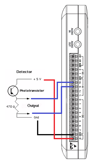
Figure 5: NI myDAQ Wiring Diagram
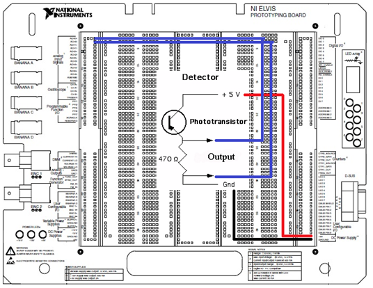
Figure 6: NI ELVIS II Wiring Diagram
*The phototransistor circuit can go anywhere on the protoboard. It was placed in the center for simplicity.
Software Instructions:
LabVIEW User Interface
The user interface we created reads the amplitude of the voltage drop across the emitter degenerating resistor, and displays the current numeric value and a waveform chart of the value over a time period.
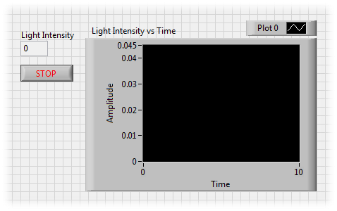
Figure 7: LabVIEW Front Panel
Coding Strategy
The LabVIEW code for the light intensity measurement is a simple two-step process, as seen below. Note that no steps are taken to convert the voltage measurement to an actual light intensity measurement, so the amplitude simply represents a relative measurement.
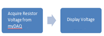
Figure 8: Coding Diagram
The LabVIEW block diagram shown below looks very similar to the coding block diagram
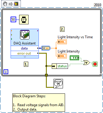
Figure 9: 'light.vi' Block Diagram
How It Works:
Inside the while loop on the left is the DAQ Assistant. It’s configured to read a single value from the myDAQ analog input 0 terminal each time it is executed. Once a value is read it is passed down the wire, converted to a useable data type, and displayed in a numeric indicator and waveform chart. All of the code inside the While Loop continues to run until the Stop button is pressed on the front panel. The Wait VI (top right) delays execution of the while loop to every 50ms. Therefore the sampling rate is 20 samples per second, or 20 Hz.
In this VI the DAQ Assistant is configured for on-demand sampling of the analog resistance input channel. The following steps walk through the configuration of the DAQ Assistant from scratch:
- Be sure your myDAQ or ELVIS II is plugged in
- Press Ctrl-Space to bring up the Quick Drop Window (takes a full minute to load on the first use)
- Search for DAQ Assistant and double click on it when it appears in the list
- Drop it on the Block diagram (white window)
- When the Create a New Express Task configuration pane appears, select
- Acquire Signals
- Analog Input
- Voltage
- Dev 1 (NI myDAQ or ELVIS II) *Note: If you have other NI hardware installed, the myDAQ or ELVIS II may not be Dev1.
- AI0
- Finish
- Change the Voltage input Setup to the correct Signal Input Range
- Max: 5
- Min: 0
- Change Timing Settings to
- 1 Sample (On Demand)
- Press OK
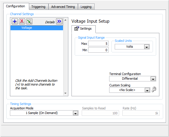
Figure 10: DAQ Assistant Frequency Configuration
*Note that sample time is set by the Wait VI and is set to sample 20 times per second (every 50ms) in this VI
Tips and Tricks:
- Move your hand up and down on top of the phototransistor while observing the waveform chart. Add a phototransmitter circuit next to the photodetector, and run the phototransmitter with the NI DAQmx Function Generator while also running the VI.
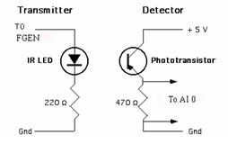
Figure 11: Phototransmitter/photodetector circuit
- You can modify the VI to log the data to file using a ‘Write To Spreadsheet File.vi’ express VI if you wish to save the data. Be sure to place it in the loop and be sure to append new data to the spreadsheet file.
References
Fundamental Photodiode Circuits
Webcasts, Tutorials, and Other How-To Resources
Learn About Relevant Training Options: Data Acquisition and Signal Conditioning
Applications Engineering
National Instruments
