- Subscribe to RSS Feed
- Mark Topic as New
- Mark Topic as Read
- Float this Topic for Current User
- Bookmark
- Subscribe
- Mute
- Printer Friendly Page
SERDES CLIP in External clock data Acquisition in Flex RIO
12-21-2017 12:45 AM
- Mark as New
- Bookmark
- Subscribe
- Mute
- Subscribe to RSS Feed
- Permalink
- Report to a Moderator
Can anyone explain the detailed structure of an SERDES Connector CLIP
in LabVIEW programming Flex RIO.
Additionally,
- How do the acquisition bits get arranged, with respect to each Channel Data?!
- How does the samples to be read considered?!!!
- If I have 16 LVDS Channels, how can I acquire each channels data considering each Lane to reconstruct separately.
Note:
I have seen examples and stuffs related to flex-rio programming but there's no particular explanation for this CLIP, Where things go in deep with high importance.
KT is worth it!! Cause you are storing things permanently in your Brain ![]()
12-21-2017 11:23 PM
- Mark as New
- Bookmark
- Subscribe
- Mute
- Subscribe to RSS Feed
- Permalink
- Report to a Moderator
Which FlexRIO and FlexRIO Adapter Module are you using?
Certified LabVIEW Architect, Certified Professional Instructor
ALE Consultants
Introduction to LabVIEW FPGA for RF, Radar, and Electronic Warfare Applications
12-21-2017 11:49 PM
- Mark as New
- Bookmark
- Subscribe
- Mute
- Subscribe to RSS Feed
- Permalink
- Report to a Moderator
Flex RIO series is PXI7966 and
Adapter module is PXI6587
01-03-2018 12:17 AM
- Mark as New
- Bookmark
- Subscribe
- Mute
- Subscribe to RSS Feed
- Permalink
- Report to a Moderator
Hello everyone,
Please help me with sorting out this problem!! ![]()
01-03-2018 12:42 AM
- Mark as New
- Bookmark
- Subscribe
- Mute
- Subscribe to RSS Feed
- Permalink
- Report to a Moderator
Have you reviewed: http://zone.ni.com/reference/en-XX/help/372614J-01/friohsdio/6587_serdesconn_clipref/
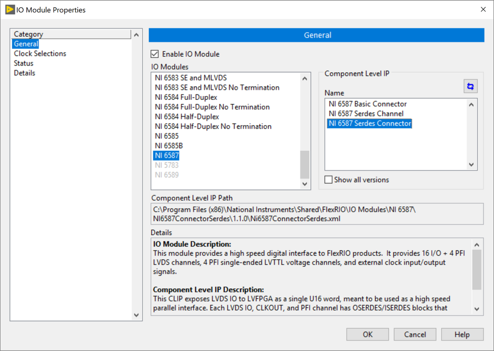
Have you reviewed the Properties of the IO Module?
Right click on IO Module >> Properties, select 6587 and on the right is a list of CLIP options:
Certified LabVIEW Architect, Certified Professional Instructor
ALE Consultants
Introduction to LabVIEW FPGA for RF, Radar, and Electronic Warfare Applications
01-03-2018 12:53 AM
- Mark as New
- Bookmark
- Subscribe
- Mute
- Subscribe to RSS Feed
- Permalink
- Report to a Moderator
Hey,
I have already read these documents and am not getting a proper idea.
In my application, the data lanes 6 to 9 are used. From which the data
is read and re-constructed for a sine wave. But, am not getting the Sine
wave. So, what I doubt now is the CLIP and in which order it sends the
data..
01-03-2018 01:25 AM
- Mark as New
- Bookmark
- Subscribe
- Mute
- Subscribe to RSS Feed
- Permalink
- Report to a Moderator
So you are unable to get the example to work?
Maybe simplify what you are trying to do? Otherwise, I would suggest reaching out to (phone) NI technical support.
Certified LabVIEW Architect, Certified Professional Instructor
ALE Consultants
Introduction to LabVIEW FPGA for RF, Radar, and Electronic Warfare Applications
01-03-2018 11:23 PM
- Mark as New
- Bookmark
- Subscribe
- Mute
- Subscribe to RSS Feed
- Permalink
- Report to a Moderator
@Terry_ALE wrote:
So you are unable to get the example to work?
Am able to make the example code work, Terr_ALE
The changes in my application, what am trying is to let a clock signal and data line, sample data with respect to the clock signal, in DDR mode. And then reconstruct, through Digital to Analog function.
Am not able to understand how to get, the detection of rising and falling edges of a clock without connecting it to Clock IN pin on the Adapter module (Cause, Signals are LVDS) or as reference.
Is this detail..?!
Thanks!!
01-04-2018 07:06 AM
- Mark as New
- Bookmark
- Subscribe
- Mute
- Subscribe to RSS Feed
- Permalink
- Report to a Moderator
I think NI technical support (phone/email) is your best route at this point.
Certified LabVIEW Architect, Certified Professional Instructor
ALE Consultants
Introduction to LabVIEW FPGA for RF, Radar, and Electronic Warfare Applications
02-22-2018 05:51 PM
- Mark as New
- Bookmark
- Subscribe
- Mute
- Subscribe to RSS Feed
- Permalink
- Report to a Moderator
Hi PriyadarsiniS,
Do you still have questions about the SERDES CLIP or were you able to create a service request to get the information you were looking for?
The documentation that Terry_Ale provided is a great place to start to understand the SERDES CLIP but if you have more questions related to your specific application, especially when modifying example code, a service request will be a better route.
Partner Development Engineer
Alliance Partner Network
National Instruments

