- Subscribe to RSS Feed
- Mark Topic as New
- Mark Topic as Read
- Float this Topic for Current User
- Bookmark
- Subscribe
- Mute
- Printer Friendly Page
Critical Path Delay using MultiSim
05-13-2020 02:19 AM
- Mark as New
- Bookmark
- Subscribe
- Mute
- Subscribe to RSS Feed
- Permalink
- Report to a Moderator
Dear Sir,
Please advise how can I find the critical path delay of a circuit using MultiSim?
05-22-2020 05:32 PM
- Mark as New
- Bookmark
- Subscribe
- Mute
- Subscribe to RSS Feed
- Permalink
- Report to a Moderator
Hello Namra26,
Could you please describe the task more detailed?
What parameters should be measured, meteorology etc..
As a starting point I think it should be done by using Transient Analysis or another tool from "Active Analysis".
Depends on task.
The best way to thank, is to give KUDOS
05-23-2020 06:05 AM
- Mark as New
- Bookmark
- Subscribe
- Mute
- Subscribe to RSS Feed
- Permalink
- Report to a Moderator
Dear Sir,
Thank your for your reply. I want to find the critical path delay of a cascaded circuit of OR gate at transistor level. I am doing transient analysis but how can I get the critical path delay by using transient analysis. What is the process to find this delay; by observing the output waveform? Please advise me some other preferable method?
I have attached the file as well.
05-23-2020 06:24 AM
- Mark as New
- Bookmark
- Subscribe
- Mute
- Subscribe to RSS Feed
- Permalink
- Report to a Moderator
So you are looking for response time between input and output?
Like how long it will take for logic gate output to respond of input state change?
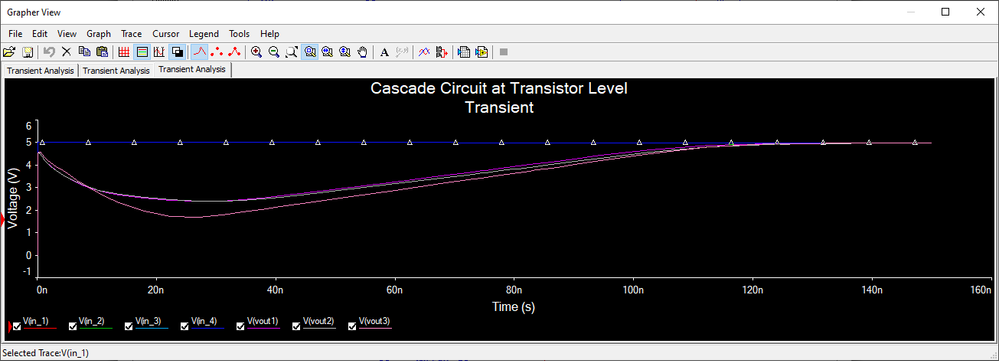
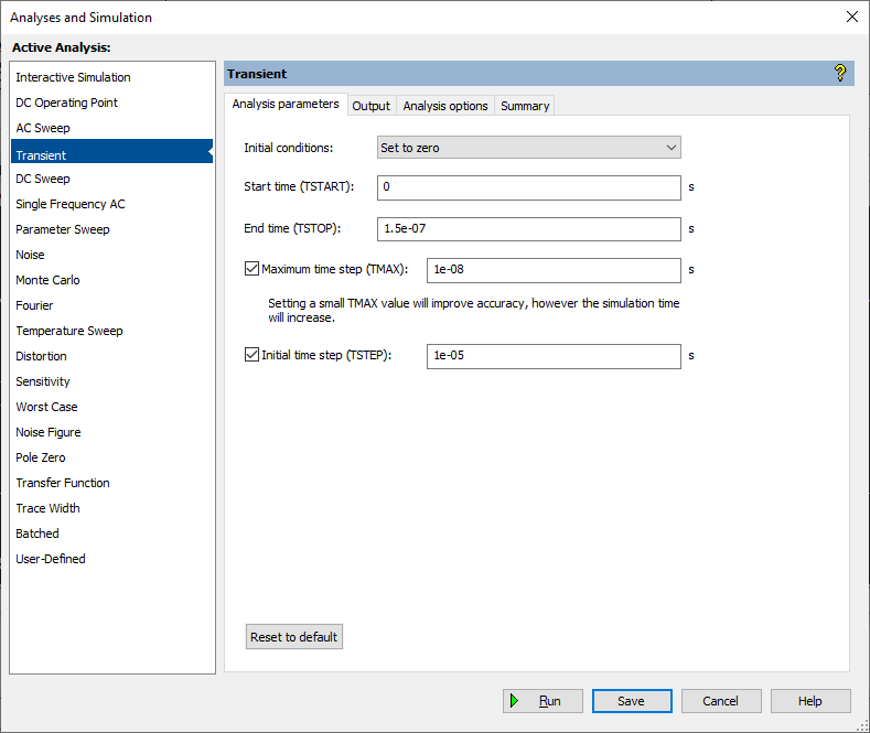
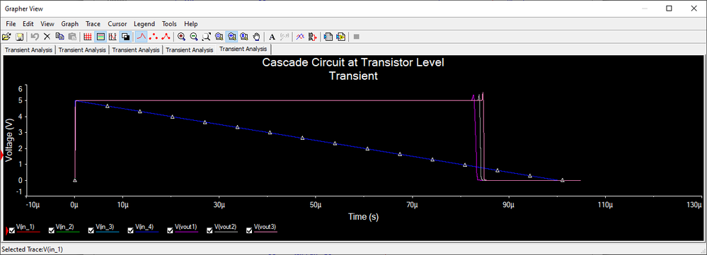
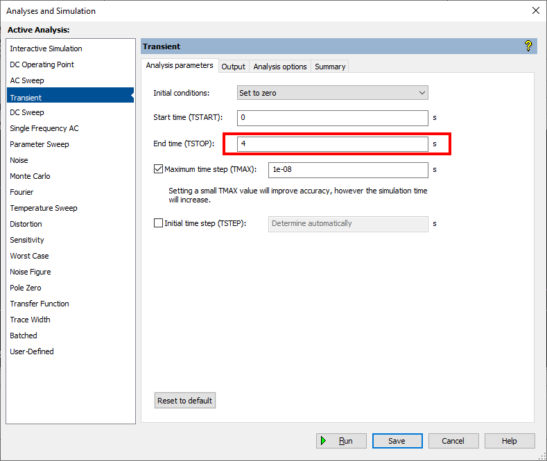
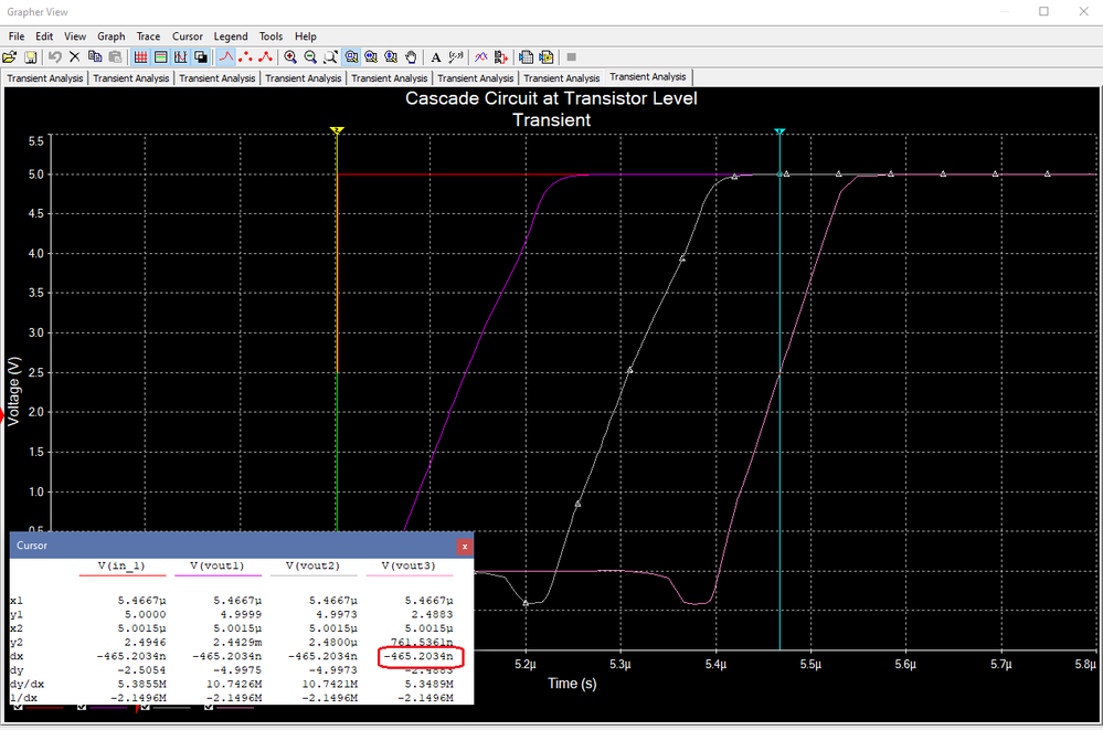
I paled with start and stop parameters, also with time stamps and here what I got.
Is this is what you are looking for?
The best way to thank, is to give KUDOS
05-23-2020 07:32 AM - edited 05-23-2020 07:34 AM
- Mark as New
- Bookmark
- Subscribe
- Mute
- Subscribe to RSS Feed
- Permalink
- Report to a Moderator
Hello, the critical path is typically the longest path between an input and an output of your circuit. This is true, unless you apply special sizing techniques for your MOSFET-s (e.g. progressive W/L, etc.). In your circuit all NMOS and PMOS transistors are identical so within a single OR gate the PMOS path is is the slowest due to much smaller carrier mobility compared to NMOS. Therefore, the critical path is from the gate of the PMOS transistor farthest from each output.
When you cascade your gates it is sufficient to apply a single rectangular voltage to the critical input (In_1) and plot the switching waveforms at each gate output. All other inputs can be simply GND as 0 is the neutral element for the OR operation. The waveforms get unnecessarily complicated if you feed periodic waveforms to the other inputs.The In_1 rectangular voltage should be fast enough, for example with period=10us, pulse width=5us and rise/fall times of 1ns to evaluate delay. With power MOSFET models used in digital logic you may need to adjust simulator options (for example reltol=0.003) to aid convergence.
By convention the delay is measured at 50% signal swing. Once you have plotted the input and output waveforms you can masure the time between the input and output 2.5V crossing (see attached plot). This time difference is your critical path delay.
06-05-2023 11:38 PM
- Mark as New
- Bookmark
- Subscribe
- Mute
- Subscribe to RSS Feed
- Permalink
- Report to a Moderator
thanks for your sharing information
