- Subscribe to RSS Feed
- Mark Topic as New
- Mark Topic as Read
- Float this Topic for Current User
- Bookmark
- Subscribe
- Mute
- Printer Friendly Page
derived clock problem?
Solved!11-22-2010 07:33 PM
- Mark as New
- Bookmark
- Subscribe
- Mute
- Subscribe to RSS Feed
- Permalink
- Report to a Moderator
I am tring to derive a 25MHz clock using a NI PXI-7842R and labview project won't allow that exact clock
But when I try doing the same thing for a PXI-7830R target, I am sucessful.
What is going on?
I am choosing a base clock of 40MHz
to get 25MHz, the multiplier is 5 and the divisor is 8
When I right click on New Derived clock, I only get the option of entering a new clock frequency.
Why does the tool not let me just specify the multiplier and divisor?
I am using Labview version 2010
Solved! Go to Solution.
11-24-2010 12:15 PM
- Mark as New
- Bookmark
- Subscribe
- Mute
- Subscribe to RSS Feed
- Permalink
- Report to a Moderator
Hi lsutiger,
This is expected behavior across various FPGA targets. Depending on the hardware resources on each of these R-series cards, they will have specific derived clock frequencies that they support. It appears that the multipliers and divisors are not able to be set directly on LabVIEW 2010, but this shouldn't be a problem since setting the clock rate has the same result. I hope this helps!
- Greg J
11-24-2010 12:54 PM
- Mark as New
- Bookmark
- Subscribe
- Mute
- Subscribe to RSS Feed
- Permalink
- Report to a Moderator
Greg,
I don't understand why particular discrete frequencies cannot be set?
Does Labview FPGA module not use Xilinx Vertex 5 DCM to set /derive clocks?
Is it possible to instantiate a DCM as component level IP (CLIP), then use that clock output as a source for a for loop for example?
Is there an example for what I am tring to do?
11-24-2010 03:20 PM - edited 11-24-2010 03:21 PM
- Mark as New
- Bookmark
- Subscribe
- Mute
- Subscribe to RSS Feed
- Permalink
- Report to a Moderator
LabVIEW FPGA does use the built-in DCMs for the Virtex 5, however, the parameters for the DCM with a 40 MHz input clock do not allow for 25 MHz on the Virtex 5.
In trying to instantiate a derived clock, there are four possible options, a 1X clock, a 2X clock, CLKDV, which is a phase-aligned clock operating at a fraction of the input clock, and CLKFX, which takes the multiplier and divisor and creates a clock of (M/D) * clock in rate.
Obviously, 1X and 2X will not work because they yield a 40 MHz and 80 MHz clock, respectively. The other two are limited by the specs for the DCM.
In looking at the Virtex-5 FPGA User Guide in the section Clock Management Technology, you will see a section for DCM Attributes. CLKDV_DIVIDE (p. 58) is an attribute set for the DCM that tells the DCM what rate the CLKDV output should run at. If you look at the available attributes, you can see that 5/8 does not fit into one of the valid configurations, so we can’t use CLKDV.
We also cannot use CLKFX because the Virtex-5 DC and Switching Characteristics Data Sheet shows that the valid ranges of CLKFX are 32 MHz to 140 MHz for the Low-Frequency Mode and 140 MHz to 350 MHz for the High-Frequency Range (p. 57). Since 25 MHz is below the minimum rate, we can't create it from this DCM output port.
You can do this on the PXI-7830R because that has a Virtex-II FPGA with different characteristics and attributes.
11-24-2010 08:29 PM - edited 11-24-2010 08:30 PM
- Mark as New
- Bookmark
- Subscribe
- Mute
- Subscribe to RSS Feed
- Permalink
- Report to a Moderator
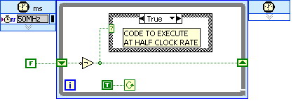
Thanks for the insight. I was trying to move towards the newer Virtex 5 FPGA since I think it will be around a lot longer than the virtex 2
Would the following scheme work for simple clocking?
Thanks Jeff
11-29-2010 09:21 AM
- Mark as New
- Bookmark
- Subscribe
- Mute
- Subscribe to RSS Feed
- Permalink
- Report to a Moderator
That should work just fine. The case structure will add a little bit of overhead to the total loop execution time, but at 50 MHz, this overhead should be minimal and you shouldn't run into many timing issues.

