- Subscribe to RSS Feed
- Mark Topic as New
- Mark Topic as Read
- Float this Topic for Current User
- Bookmark
- Subscribe
- Mute
- Printer Friendly Page
Receive high speed ADC output data with Labview FPGA
07-04-2019 09:46 AM
- Mark as New
- Bookmark
- Subscribe
- Mute
- Subscribe to RSS Feed
- Permalink
- Report to a Moderator
Hello,
I'm using sbRIO9651 to receive outputs data of ADC (LTC2174) with Labview FPGA.
I have a question about it:
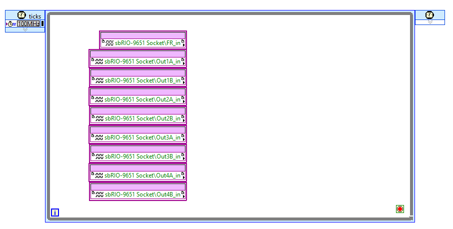
The data clock output (DCO) of ADC is 400MHz. If I use a SCTL with a 100MHz clock which is derived from DCO, for data acquisition (see the picture), the data outputs will at each iteration export more data bits or just at one iteration export one bit?
07-04-2019 02:53 PM
- Mark as New
- Bookmark
- Subscribe
- Mute
- Subscribe to RSS Feed
- Permalink
- Report to a Moderator
07-04-2019 04:56 PM - edited 07-04-2019 04:58 PM
- Mark as New
- Bookmark
- Subscribe
- Mute
- Subscribe to RSS Feed
- Permalink
- Report to a Moderator
Hi GerdW,
thanks for your reply. You mean each data output exports one boolean value at each iteration?
If so, how can I receive all boolean values of each output without data loss? The DCO(400MHz) is too fast, so I can't directly use it as the iteration clock of SCTL. But except SCTL, I don't know if there are other ways to receive the data at this high speed.
Best regards,
John
07-04-2019 05:10 PM
- Mark as New
- Bookmark
- Subscribe
- Mute
- Subscribe to RSS Feed
- Permalink
- Report to a Moderator
When the clock rate is slower than the rate of the I/Os, LabVIEW FPGA has multiple I/Os e.g. AI0N, AI0N-1, AI0N-2, AI0N-3 (or similar).
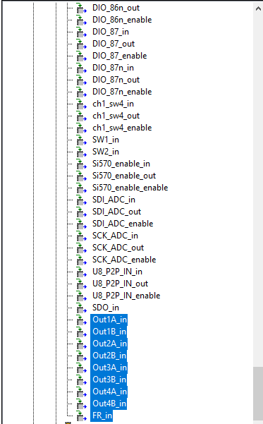
By reading these, you get parallel data which allows you to maintain the throughput. I am not familiar with this card or your config. Could you post screenshots of the pin outs under the Socket from the project (or post the project)?
Certified LabVIEW Architect, Certified Professional Instructor
ALE Consultants
Introduction to LabVIEW FPGA for RF, Radar, and Electronic Warfare Applications
07-05-2019 04:27 AM
- Mark as New
- Bookmark
- Subscribe
- Mute
- Subscribe to RSS Feed
- Permalink
- Report to a Moderator
Hi Terry,
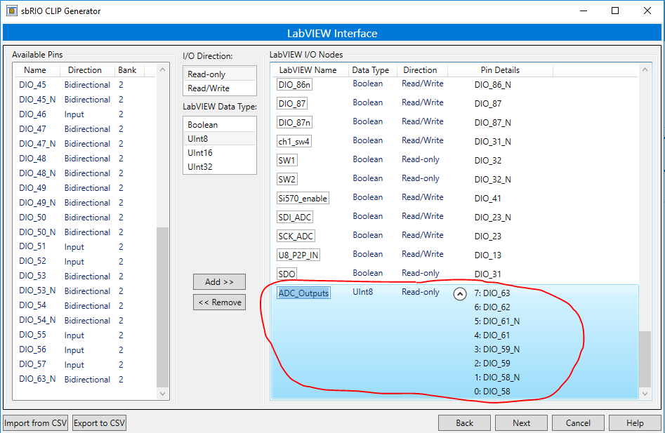
you mean configure all data outputs as one I/O node with sbRIO CLIP Generator, e.g. UInt8 type (like picture 1)?
This can truly make each output parallel exporting data. But the data rate of each output is still same as before and is faster than the clock of SCTL. So there will also be data loss.
The physical connection form between ADC outputs and FPGA I/O is: Each ADC output lane (Out1A, Out1B...Out4B) is connected to one DIO of FPGA. When ADC is working, each output lane will export data bit (boolean value) at 400MHz DCO.
Picture 2 is the current pin under Socket from the project. In the attachment it's project files. Could you have a look at them. Thanks.
Best regards,
John
07-05-2019 11:46 AM
- Mark as New
- Bookmark
- Subscribe
- Mute
- Subscribe to RSS Feed
- Permalink
- Report to a Moderator
Not like picture 1.
I do not use sbRIO but I have worked with other NI FPGA hardware that runs at higher the rate of the SCTL. Besides the sbRIO-9651 http://www.ni.com/pdf/manuals/376962c.pdf what other hardware are you using? I am unable to find the reference to the 400 MHz DCO.
Certified LabVIEW Architect, Certified Professional Instructor
ALE Consultants
Introduction to LabVIEW FPGA for RF, Radar, and Electronic Warfare Applications
07-09-2019 03:51 AM - edited 07-09-2019 03:54 AM
- Mark as New
- Bookmark
- Subscribe
- Mute
- Subscribe to RSS Feed
- Permalink
- Report to a Moderator
Hi Terry_ALE,
sorry for the delayed reply. sbRIO 9651 is the first NI hardware that I used for development work. Now I'm trying to reduce the sampling rate of ADC, then DCO of ADC will also be automatic reduced. In this way, I think Labview can handle it better under a slower rate. Thanks for your help.
Best regards,
John

