- Subscribe to RSS Feed
- Mark Topic as New
- Mark Topic as Read
- Float this Topic for Current User
- Bookmark
- Subscribe
- Mute
- Printer Friendly Page
[FPGA] Tick Wait vs Discrete Delay not adding up
05-27-2015 09:29 AM
- Mark as New
- Bookmark
- Subscribe
- Mute
- Subscribe to RSS Feed
- Permalink
- Report to a Moderator
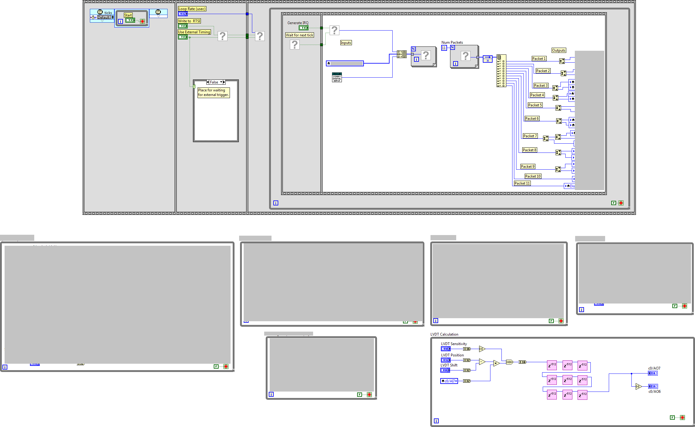
We have found a solution to an offset problem between 2 sine waves, however we are unable to explain the delay calculations... (Someone else did the work a long time ago, now we need to explain the fix).
(All information displayed in image below)
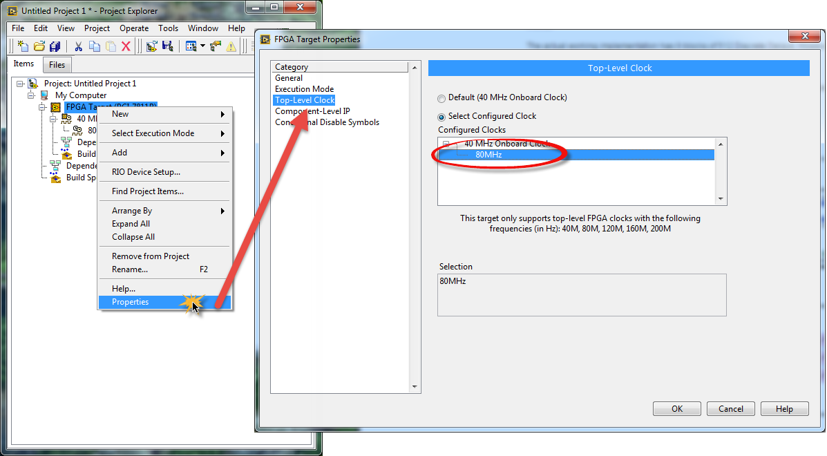
The FPGA derived is at 80MHz.
There's 6us delay between the input Sinewave and the generated Sinewave from that input. Sinewave period is 416us.
The initial reasoning was to put a 404 Tick delay (The way it was added is wrong of course). But 404 Tick delay is still calculable: 404*(1/80MHz) = 5.05us
The actual working implementation has 9 blocks of 512 Discrete Delays. However this calculation is not adding up in any way to the 6us (or even 410us delay for the initial period to be lost).
9*512*(1/80MHz) = 57.6us.
The system automatically detects if there is an error greater than 5 degrees phase shift.
Are my calculations wrong?
Thanks 🙂
05-28-2015 04:18 AM
- Mark as New
- Bookmark
- Subscribe
- Mute
- Subscribe to RSS Feed
- Permalink
- Report to a Moderator
The upper loop with the 404 Tick delay does nothing to help your cause, it simply slows down your output. I'm not surprised your delay didn't change with this code.
How do you arrive at your 6us delay in your sive wave? Is it measured? Are you sure the 57.6 us isn't actually correct? Are you absolutely sure the code is running at 80MHz? Usually for a timing like that you would use a timed while loop, not a normal while loop.
Shane
05-28-2015 05:16 AM - edited 05-28-2015 05:17 AM
- Mark as New
- Bookmark
- Subscribe
- Mute
- Subscribe to RSS Feed
- Permalink
- Report to a Moderator
Your output needs to be delayed by 410us (not 6).
As the previous poster said, you need to be using a timed loop.
If it's all working,
9*512*(1/loop_rate)=410 E-6
loop_rate=9*512/(410 E -6)=1.1239 E 7 Hz or 11.239 MHz
80/11.239=7.11
Is your loop actually running at a derived 80/7? That would make sense of the result.
05-28-2015 05:49 AM
- Mark as New
- Bookmark
- Subscribe
- Mute
- Subscribe to RSS Feed
- Permalink
- Report to a Moderator
ToeCutter wrote:
Is your loop actually running at a derived 80/7? That would make sense of the result.
No, it just takes 7 ticks to run an iteration of the loop. We are not in a SSTL, so each operation in there takes at least 1 tick. I quickly added up 7 ticks (whith the loop iteration).
There are only two ways to tell somebody thanks: Kudos and Marked Solutions
Unofficial Forum Rules and Guidelines
"Not that we are sufficient in ourselves to claim anything as coming from us, but our sufficiency is from God" - 2 Corinthians 3:5
05-28-2015 08:11 AM
- Mark as New
- Bookmark
- Subscribe
- Mute
- Subscribe to RSS Feed
- Permalink
- Report to a Moderator
The 6us delay on the sinewave is measure with a scope
How can I know what the code is running at? I assume that it is based on the derived 80MHz that is shown in the project.
The code cannot be modified.
Thanks
05-28-2015 08:24 AM
- Mark as New
- Bookmark
- Subscribe
- Mute
- Subscribe to RSS Feed
- Permalink
- Report to a Moderator
If the other loops could affect the questioned loop, here is the complete code censored (The missing VIs are from NI VeriStand Lib).
Thanks
05-28-2015 08:28 AM
- Mark as New
- Bookmark
- Subscribe
- Mute
- Subscribe to RSS Feed
- Permalink
- Report to a Moderator
You have, in your original images, an Analog Input and an Analog Output shown. Which is which in the oscilloscope trace? Have you factored in any hardware delays into your considerations? In my experience, hardware delays can often exceed the implemented software delays and certainly need to be taken into account when dealing with this kind of thing. How long does it take for an AO signal to leave the FPGA code and return via Input? This can be tested by running a simply ramp and comparing the signals on the FPGA.
05-28-2015 09:33 AM
- Mark as New
- Bookmark
- Subscribe
- Mute
- Subscribe to RSS Feed
- Permalink
- Report to a Moderator
The purple trace is the input and the orange trace is the output. We have not considered hardware delays as we planed to adjust the delay experimentally. The analog in signal is not feedback from the analog out but the control signal from the UUT.
How can I know what the code is running at? I assume that it is based on the derived 80MHz that is shown in the project. How does 9 X 512 get aprox 410usec?
05-28-2015 09:51 AM
- Mark as New
- Bookmark
- Subscribe
- Mute
- Subscribe to RSS Feed
- Permalink
- Report to a Moderator
You can determine the top-level (default) clock by looking in the FPGA target properties.
05-28-2015 09:55 AM
- Mark as New
- Bookmark
- Subscribe
- Mute
- Subscribe to RSS Feed
- Permalink
- Report to a Moderator
You are reading in a signal from a device via ADC and then want to output a time-delayed signal where the overall delay is 6 us, right? So your FPGA is simply a programmable delay circuit in this case? Have I understood this correctly?
Try outputting your AI (signal from your UUT in FPGA-space) directly to a seperate AO without going through the discrete delays so that you are outputting both the delayed and the non-delayed signal. Then use your oscilloscope to look at all three signals:
1) the raw signal from your UUT
2) the "raw" output
3) the delayed output.
Differences between 1 and 2 are hardware delays. Differnces between 2 and 3 are due to the discrete delay blocks you are trying to understand.
If you want to know what speed the code is running at try bit flipping a boolean in each case and then write it to a high-speed digital line. Looking at the result on an oscilloscope will give you the rate.


