- Subscribe to RSS Feed
- Mark Topic as New
- Mark Topic as Read
- Float this Topic for Current User
- Bookmark
- Subscribe
- Mute
- Printer Friendly Page
- « Previous
-
- 1
- 2
- Next »
Speed of reading "Read/Write control" on FPGA
08-22-2018 04:37 PM
- Mark as New
- Bookmark
- Subscribe
- Mute
- Subscribe to RSS Feed
- Permalink
- Report to a Moderator
1. It's a front panel control on the FPGA.
2. Yes, the 2nd loop simply - writes from one FPGA Front panel control to another via a local variable.
3. I would suppose during bitfile deployment, what RT Front panel 'link' resources are required - if there is no call - it does not deploy them. And that 'un-RT' linked control on the FPGA FP - does not bother to check for FP updates..and runs on it's merry way...
08-22-2018 05:38 PM
- Mark as New
- Bookmark
- Subscribe
- Mute
- Subscribe to RSS Feed
- Permalink
- Report to a Moderator
@MrJackHamilton wrote:
1. It's a front panel control on the FPGA.
2. Yes, the 2nd loop simply - writes from one FPGA Front panel control to another via a local variable.
3. I would suppose during bitfile deployment, what RT Front panel 'link' resources are required - if there is no call - it does not deploy them. And that 'un-RT' linked control on the FPGA FP - does not bother to check for FP updates..and runs on it's merry way...
There's clearly some misunderstanding here. Any chance we can see some of your code? I have, many times, put a front panel control in a single-cycle loop on an FPGA, and I don't get timing errors, meaning that it reads from the front panel control on every FPGA clock cycle. I've never needed a separate loop for copying to a local variable. The FPGA bitfile doesn't get adjusted on the fly as it's deployed, never mind that you can deploy a single bitfile and run it directly on the FPGA, bypassing the RT component, then run the same FPGA within an RT application without re-deploying.
08-22-2018 06:57 PM
- Mark as New
- Bookmark
- Subscribe
- Mute
- Subscribe to RSS Feed
- Permalink
- Report to a Moderator
nathand,
I did not infer there would be 'timing errors' or errors posted of any kind from the FPGA or the RT. We were doing nanosecond high-speed timing and had the gear to measure the pulse outputs electrically. We saw a long latency in the digital pulse train, when we push a different pulse width, this clearly was from the 'transaction' between the RT and FPGA. Where were using the 55nsec High-Speed digital output module [9402].
Don't know how long the time was, it was not insanely long..maybe 100's of picoseconds.
You'd not see it with most applications, frankly unless your looking, or recording while changing settings. We just happened to be.
I don't believe that there is any statement about the FPGA reading an FP control in a single clock-cycle. Additionally, many of the C-series modules, take more than one clock cycle on Reads and/or writes in the FPGA. You'd need to cycle time the FPGA loops to discover this. I would offer you should always drop in a loop cycle time rate in your FPGA loops to understand the actual timing. Too much logic or other operations; can take N-clock cycles.
This is similar to front panel updates on Windows - where there is some negotiation as to when the control value is changing - then changed - then the change propagated thru the code.
I can call up the code and post some pics...when I find it in my archives.
Regards
Jack Hamilton
Regards
Jack
08-22-2018 07:25 PM
- Mark as New
- Bookmark
- Subscribe
- Mute
- Subscribe to RSS Feed
- Permalink
- Report to a Moderator
@MrJackHamilton wrote:
I did not infer there would be 'timing errors' or errors posted of any kind from the FPGA or the RT. We were doing nanosecond high-speed timing and had the gear to measure the pulse outputs electrically. We saw a long latency in the digital pulse train, when we push a different pulse width, this clearly was from the 'transaction' between the RT and FPGA. Where were using the 55nsec High-Speed digital output module [9402].
and quoting your previous post:
@MrJackHamilton wrote:Why?: Because when you place a control/parameter in an FPGA loop - THAT IS DIRECTLY CONNECTED TO THE RT - it carries with it lots of overhead - essentially, you're asking that FPGA loop to simultaneously 'check' up with the RT if the value changed. This creates a huge lag - I've seen this on scope traces with the high-speed digital module - when we changed the timing parameters from the RT.
Absolutely there's overhead transferring from the RT to the FPGA, but my point was that the overhead is entirely on the RT side. As far as the FPGA is concerned, the front panel controls are registers that the RT side can set. The FPGA doesn't "check up" to see if the value changed; it just pulls the latest value from the register on each loop iteration. That process takes the same amount of time, or at least the same number of clock cycles (as I mentioned, it can be done consistently within a single clock cycle), regardless of whether there is an RT process connected to the FPGA.
I'm not doubting that you solved some problem by adding in another loop, but maybe I've misunderstood what problem you solved, since I cannot see any reason that adding in an additional transfer loop would make it faster to move data between the RT and FPGA through front-panel controls.
08-23-2018 03:48 AM
- Mark as New
- Bookmark
- Subscribe
- Mute
- Subscribe to RSS Feed
- Permalink
- Report to a Moderator
I agree that this sounds like some misconceptions are present.
Are the two loops you refer to controlled by the same clock? If so, then what you have done is equivalent to just adding a single feedback node to the reading of the FP control.
Are you using SCTLs? For both FP reading AND your device control?
08-24-2018 03:55 PM
- Mark as New
- Bookmark
- Subscribe
- Mute
- Subscribe to RSS Feed
- Permalink
- Report to a Moderator
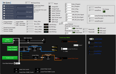
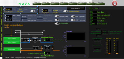
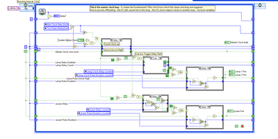
Ok, I dug the code up from my archives, here are some FP and FPGA Code Diagram screenshots. As you can see it was to provide timing/pulse control for a pulsed laser.
[Above] RT Front Panel - which for R&D we ran the RT Front panel.

[Above] FPGA Front panel - same as RT - as we want to clearly communicate to the Laser R&D scientists what exactly is going on with the timing and pulse/timing settings. (They liked this GUI very much - very clear to understand.
[Above] The FPGA Pulse Timing loop - this is where the timing settings were modified from the RT FP, notice - No FPGA I/O nodes here - they read the 'Lamp Fire' controls via the local variables in this loop.
Again: This was a recommended implementation from NI - which WORKED exceptionally well. As the conventional coding method - FPGA FP controls in the same loop as FPGA I/O calls - cause long observed latency...via a oscope on the laser pulse control lines.
Regards
Jack Hamilton
08-27-2018 09:36 AM
- Mark as New
- Bookmark
- Subscribe
- Mute
- Subscribe to RSS Feed
- Permalink
- Report to a Moderator
@MrJackHamilton wrote:.Again: This was a recommended implementation from NI - which WORKED exceptionally well. As the conventional coding method - FPGA FP controls in the same loop as FPGA I/O calls - cause long observed latency...via a oscope on the laser pulse control lines.
Still seems fishy to me. I have had DIO modules running at 40MHz inside of a SCTL with no issues at all. Maybe your issues are related to your derived clock?
And I am hoping that code was sanitized. There are a lot of Rube Goldbergs in there (Equals True can just be a wire, Equals False can just be a NOT, etc)
There are only two ways to tell somebody thanks: Kudos and Marked Solutions
Unofficial Forum Rules and Guidelines
"Not that we are sufficient in ourselves to claim anything as coming from us, but our sufficiency is from God" - 2 Corinthians 3:5
08-27-2018 11:56 AM
- Mark as New
- Bookmark
- Subscribe
- Mute
- Subscribe to RSS Feed
- Permalink
- Report to a Moderator
I should note this was over 6+ years ago, and was an early version of cRIO FPGA/RT. [I also stay one year back from the current dev ver of LV] Which as we know, things get better over time.
- « Previous
-
- 1
- 2
- Next »


