- Subscribe to RSS Feed
- Mark Topic as New
- Mark Topic as Read
- Float this Topic for Current User
- Bookmark
- Subscribe
- Mute
- Printer Friendly Page
Digital Line Input and Output (R series)
01-10-2020 06:02 PM - edited 01-10-2020 06:04 PM
- Mark as New
- Bookmark
- Subscribe
- Mute
- Subscribe to RSS Feed
- Permalink
- Report to a Moderator
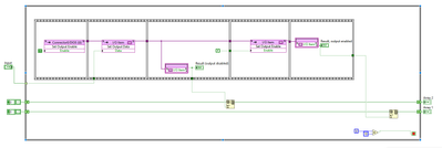
Hi, I wanted to go through the Digital Line Input and Output - R Series project (this is available if you open LabVIEW > Help > Find Examples -> Search Tab -> type in digital input and the project Digital Line Input and Output - R series should be one of the first few searches). I feel like it's not working - I may be wrong. Either way, I'd like to understand this because I am currently trying to implement a LabVIEw FPGA code where I write into 4 separate DIO ports in each clock cycle as well as read from them. I was going to write and read from those ports as shown in this example, but I don't think the example is working. I've also read the recommended Using FPGA I/O (FPGA Module).
All I want to do is write a value into a DIO connector such that the value is truly being output there in the hardware and I can look at it in using an oscilloscope by using that DIO port. That's the ultimate goal. Now the intermediate goal was for me to verify that when I write the data into the node, I can also read it and see that it is truly there and was written there.
I've tried a number of things. The document mentioned to write the data before you enable the output so that when the output is enabled the data you write is output.
This means: FPGA I/O Method Node: Set Output Enable to False --> Set Output data to Data value that you want --> FPGA I/O Method Node: Enable True --> FPGA I/O Node and wire an indicator at the output. This does not work. I've tried different ways (such as enabling the output first), I used a flat sequence structure, etc. The values come out randomly and I can't figure out where they are coming from. They also look different at each iteration even though I'm trying to write in the same data. I am very confused. If anyone understands this better let me know.
01-10-2020 10:57 PM
- Mark as New
- Bookmark
- Subscribe
- Mute
- Subscribe to RSS Feed
- Permalink
- Report to a Moderator
@thej178 wrote:
I've tried a number of things. The document mentioned to write the data before you enable the output so that when the output is enabled the data you write is output.
This means: FPGA I/O Method Node: Set Output Enable to False --> Set Output data to Data value that you want --> FPGA I/O Method Node: Enable True --> FPGA I/O Node and wire an indicator at the output. This does not work. I've tried different ways (such as enabling the output first), I used a flat sequence structure, etc. The values come out randomly and I can't figure out where they are coming from. They also look different at each iteration even though I'm trying to write in the same data. I am very confused. If anyone understands this better let me know.
What you want to do doesn't make any sense. That is not the way a DIO line works. You need to set it to either an input or output. Then you proceed to write a value if you make it an output, OR read a value if you made it an input. It sounds like you are trying to turn the pin into a two way street where you are reversing direction at will and expect that is somehow holds onto a value for you. The pin is not some sort of storage spot. It is just a connection to the outside world and the input/output setting is just to decide whether you want to read a voltage that is being sourced from the outside world, or to output a voltage that is being sourced from the RIO (or controlled by sinking the outside voltage, depending on the type of output.) If you are outputting a voltage, there is no need for you to read from them because you know what value you had output to them.
Unless you are trying to create some bidirectional port like those that exist for 2-wire RS-485. Those usually have a third state that they can set between the input and output modes. I believe that involves more circuitry than what would exist in the DIO pins of the R series card. If I'm mistaken, then I hope someone points that out so that I can learn something new.

