Overview
This example was written to provide fast data interchange between Compact RIO targets using just available digital lines. Using one line from NI 9401 modules in two chassis it can reliably transfer 2 MB/s continuously. The same code will work over any digital line, just the speed will change.
Description
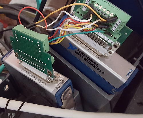
Having a situation where we needed access to data from a second FPGA target directly from the first, I began to think of a simple way of exchanging data. There are serial commumnication examples, or even SPI or IIC but they require specific hardware capabilities and, critically, the availability of several spare DIO lines. We had several slave devices and so needed to minimise DIO lines and dependencies.So, how to pass the data around? Well, firstly it was tried with a clock and data pin. This turned out to be wasteful of the available bandwidth and would have required an extra module for our application. Thinking back to this communication example I was encoding the data into the time between triggers. Given the maximum switching rates of the DIO lines, it then occurred that we could simply encode the data into the time between transitions on a digital line. Unlike the case with the NI 9469, there is no re-arm overhead to account for and so it is much simpler.Taking an inbound FIFO of U64s, the FPGA Send Data VI waits until something is available. Then it encodes the bits into the delays between switching the state of a chosen DO line. It does this after either "Tick Resolution" ticks of the chosen clock for a logic 0 or twice that for a logic 1. On completion of the last interval we have a delay of at least twice that of logic 1. This resets everything in the FPGA Receive Data VI, particularly if the connection is made mid-transmission.The FPGA Receive Data VI takes the same arguments but pushes the received data out into a FIFO. It waits on transitions and if it decodes correctly for 64 bits, the number is pushed into the FIFO and the receive loop is reset. If it sees a transition that is too long, the process is reset.Note that in the example, I am using a 120 MHz derived clock. All of the direct DIO devices can talk to the io lines very much faster than the rate in the module or card specs. Those relate to the minimum time for a transition to be guaranteed to register and to achieve the full voltage swing on the output. In this case I'm querying or setting the line on a NI 9401 at 120MHz but certainly not changing it's state at that rate. The advantages from doing this stem from the requirement to talk between devices running on separate base clocks. If I just used the 40MHz base clock on each, then at some point, the receiver would be just ahead of the transmitter. It would be easy to miss data or find that the input had not yet charged sufficiently to register. Running everything on a faster clock, we can check the state more frequently - three times per cycle minimum.Anyway, I was using 120MHz, but you can use the same VIs with any rate you like (and can get away with). Don't reduce the "Tick Resolution" below 3 though, for the reasons stated above.Another consideration was whether to include any parity checks or the like. This would have made the code more cumbersome though and much more complicated to integrate into an application. I'm using U64s as data can be packaged with information about its origin before being added to the outbound FIFO. If checksums etc really are needed, then add them into some spare space in the U64.In testing I failed to capture any instances of data loss or corruption. I was running the code on two cRIOs (a 9039 and a 9022 with a 9118 chassis) each with a NI 9401 in slot 8. I had wired pin to pin all of the lines but was just using one line inbound and one out. See picture below for the scruffy, unshielded cabling used. Data throughput was above 2 MB/s.One thing to note here is that the data takes a variable amount of time to send, with 0XFFFFFFFF taking almost twice that of 0x000000000xFFFFFFFF would take 2 x 3 x 64 + 4 * 3 = 396 ticks of the 120 MHz clock. That equates to 303k U64s per second or 2.4 MB/s.
Requirements
Software
- LabVIEW Full or Professional Development System 2012 (or compatible)
- LabVIEW Real-Time Module 2012 (or compatible)
- LabVIEW FPGA Module 2012 (or compatible)
Hardware
- Two Compact RIOs with FPGA and Real-Time target (e.g. cRIO 9024 or compatible)
- Digital I/O C Series Module in each Compact RIO (e.g. NI 9401 or compatible)
Steps to Implement or Execute Code
- Download and extract the attached file "DIO Data Transfer LV2012 NIVerified.zip".
- Follow the instructions in Real-Time and FPGA Front Panel and Block Diagram and run the Real-Time VI.
- I've included just one target chassis but you will need two to test this properly. You can use just the one and loopback the digital line but this is not representative as the single chassis will not exhibit the clock drift seen between two chassis.
- The rest is fairly self-evident.
- If running the Send and Receive VIs interactively, do be aware that the chart updates don’t relate to the the whole dataset being passed through as they don’t update like that. Even when no dat is being received they will appear to update but it’s just the way the display side connects to the FPGA code. Check this by passing the data back to the host if you are unsure.
Additional Information or References
FPGA Send Data:

FPGA Receive data:

FPGA test VI that shows how to use sender and receiver:

Real-Time VI test VI:

Test cabling between modules:
**The code for this example has been edited to meet the new Community Example Style Guidelines. The edited copy is marked with the text ‘NIVerified’. Read here for more information about the new Example Guidelines and Community Platform.**
