Multi-module Multirecord Acquisition with Reconfigurable Scope Devices Example
- Subscribe to RSS Feed
- Mark as New
- Mark as Read
- Bookmark
- Subscribe
- Printer Friendly Page
- Report to a Moderator
Products and Environment
This section reflects the products and operating system used to create the example.To download NI software, including the products shown below, visit ni.com/downloads.
- PXIe-5170
- PXIe-5171
- PXIe-5172
- PXIe-6674T
Hardware
- LabVIEW
Software
- NI-SCOPE
Driver
- Windows
Operating System
Code and Documents
Attachment
Description
Description-Separate-1This example will demonstrate the synchronization capability of multiple reconfigurable scope devices (PXIe-5170/1/2) using the PXIe-6674T timing card in a PXI chassis. A software start trigger is used to start the synchronous acquisition.
The example is built using the standard ‘Multirecord Acquisition’ sample project, modification to the FPGA target is possible, users can add inline DSP and make use of the general purpose PFI lines that are only accessible from the FPGA on these devices.
The HW setup for this demo consists of a PXIe-6674T card in the timing slot of a PXI chassis, and arbitrary number of PXIe-517x cards in the other slots. It is advised to take care of proper thermal management considerations, keep the chassis’ fans on high and leave spacing between the cards.
The example code was tested with PXIe-5170/1 cards in combination, with a maximum of 4 ns delay between the acquisitions.
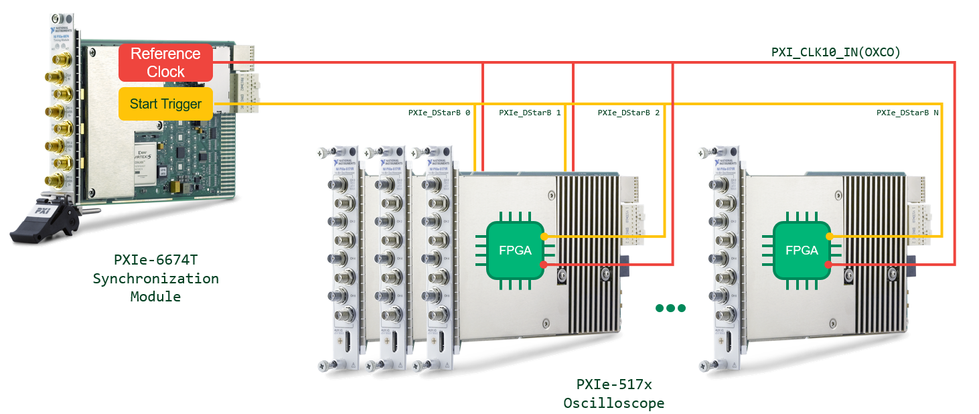
Connection Diagram of PXIe-517x Synchronization
The connection diagram above describes the architecture of this application. The timing device shares its onboard OCXO clock to the PXI backplane, so each scope can derive their sample clock from the same clock source. The start trigger for the acquisition is also shared from the PXIe-6674T card, using the ‘DStarB’ trigger lines.
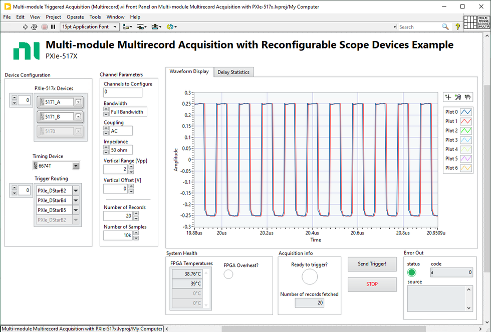
Main VI Front Panel – Waveform Display
After downloading the attached zip ('Multi-module multirecord acq w 517xR.7z'), open the LabVIEW project and open ‘Multi-module Triggered Acquisition (Multirecord).vi’ in the project tree. You can either build the FPGA bitfile under the FPGA target, or download the appropriate bitfile zip and add it to the FPGA Open VI on the block panel (marked with comment 5).
Set the devices in the appropriate controls, and also setup the proper ‘DStarB’ trigger lines to each of the PXIe-517x modules in your system. Information regarding trigger routing can be found in the user manual of your PXI chassis, there is an example picture taken from the user manual of PXIe-1085.
Trigger routing for PXIe-1085 chassis
Configure the channel parameters and start the VI. Make sure to click ‘Send Trigger!’ after the ‘Ready to Trigger?’ indicator turns on, to start the synchronous Multirecord acquisition.
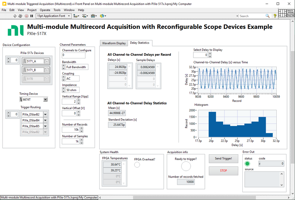
To get a better understanding about the accuracy of the acquisition, switch to the ‘Delay Statistics’ tab, to get results from delays of adjacent channels, and further statistical analysis such as chart display and histogram.
Main VI Front Panel –Delay Statistics
This example was tested using the following devices:
- PXIe-1085
- PXIe-8135
- PXIe-5170R
- PXIe-5171R
- PXIe-6674T
This example was tested using following LabVIEW / driver versions:
- LabVIEW 2020 SP1 (64-bit)
- NI-SCOPE 20.7
- NI-Sync 20.1
Description-Separate-2
Example code from the Example Code Exchange in the NI Community is licensed with the MIT license.


