- Document History
- Subscribe to RSS Feed
- Mark as New
- Mark as Read
- Bookmark
- Subscribe
- Printer Friendly Page
- Report to a Moderator
- Subscribe to RSS Feed
- Mark as New
- Mark as Read
- Bookmark
- Subscribe
- Printer Friendly Page
- Report to a Moderator
digsys-08: Design Case Study: Reaction Timer Electronics for a Children’s Museum Exhibit
Introduction
The capstone project in an introductory digital circuits and systems course provides students with an opportunity to apply register transfer level (RTL) and controller/datapath partition design techniques to solve a practical and interesting problem. This article presents a design case study for an example capstone project to design the electronics module for a children’s museum “reaction timer” exhibit. Previous articles in this series presented the techniques necessary to develop an FPGA-based solution to this design problem with LabVIEW FPGA, and will be referenced at appropriate points.
The design case study begins with the specifications provided by the museum exhibits coordinator, and then proceeds through each step of the design process: start with a generic system model composed of a controller and a datapath, develop the high-level system block diagram, design the details of the datapath components, create a state diagram for the system controller, verify the complete system with a desktop-targeted VI called the “design verification model” (DVM), re-target the DVM to an FPGA development board, and verify the FPGA-based system.
The reaction timer targets both the Xilinx Spartan-3E Starter Kit and the National Instruments Digital Electronics FPGA development boards. The Starter Kit version takes full advantage of the 16x2 character LCD for the numerical display. Refer to the links section at the end of this article for the LabVIEW project files and all other VIs discussed in this article.
The following video demonstrates the finished reaction timer project operating on the Xilinx Spartan-3E Starter Kit board:
A new exhibit under development at a local children’s museum educates visitors about the neurology of the human body. One of the exhibit stations features a hands-on activity in which the child reacts as quickly as possible to an optical stimulus, thereby quantifying the reaction time of his or her eye-to-brain-to-muscle neuro-pathway. The following diagram shows a concept drawing for the physical layout of the “reaction timer” station:
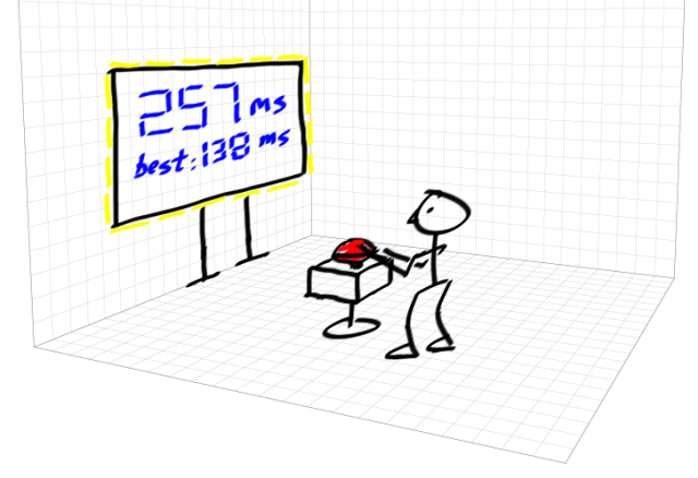
The display pod features a large three-digit numerical display for the primary reaction time measurement, a value between zero and 999 milliseconds. A smaller numerical display shows the best (shortest) reaction time recorded so far. Light stripes – arrays of LEDs – encircle the display pod and serve as the optical stimulus. The smaller button pod sports a large palm-sized “mushroom head” pushbutton that stops the timer.
The exhibits coordinator requests that a custom electronics module be developed for this reaction timer station with the following behavior:
1. When idle, the station will display the most recent reaction time measurement as well as the best time recorded so far (a hidden reset button returns the best time to “999”); the light stripe will show a medium-speed pattern that attracts interest to the station;
2. When a child presses the pushbutton, the reaction time display clears to 0 ms and the light stripe shows a slow-speed pattern of short-duration pulses to indicate “get ready”;
3. After the child releases the pushbutton, the reaction timer waits for a random time interval (roughly between 3 and 10 seconds) and continues to show the slow-rate pattern on the light stripe. Pressing the pushbutton again during this waiting interval causes the reaction timer to return to Step 2 – this prevents the guest from simply holding down the button during the wait interval and achieving a reaction time of 0 seconds;
4. Once the random wait time expires, the light stripe flashes a high-speed “GO!” pattern and the millisecond timer commences;
5. Pressing the pushbutton stops the millisecond timer and returns the reaction timer to its idle state (Step 1)
The exhibits coordinator also requests flexibility for the electronics module so that the reaction timer’s behavior can be changed easily. An FPGA development board will serve as the main hardware platform; another designer will add power transistors and cables to drive the light stripes. For this first development pass, the eight LEDs of FPGA development board will suffice to show the intended behavior of the light stripes which contain closer to 100 LEDs.
Step 1: Start the design with a generic controller/datapath system model
The design process for many digital systems partitions the system into a two distinct components: a data-oriented device (also called a datapath) and a control-oriented device (also called a controller) as depicted below:
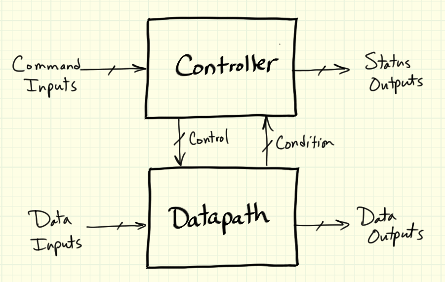
The datapath stores and manipulates information in a useful way. The controller manages the datapath by responding to conditions (such as divide-by-zero error) and deciding what operations to perform next. The datapath and controller have complementary sets of advantages and disadvantages. The controller, normally implemented by a state machine (details at State Machines for FPGA-Based Controllers), excels at decision-making and scheduling activities that occur and possibly change over time. A standard template of next-state decoder, state register, and output decoder defines the state machine hardware, therefore a state diagram captures the unique controller behavior for a given system.
State machines become cumbersome with too many states, however. For example, an 8-bit counter implemented by a state machine requires at least 256 distinct states. On the other hand, implementing an 8-bit counter in a datapath is routine. Datapath structures can handle large and complex data management tasks, but need help to know what task is required at what time. Therefore dividing a given design task into a controller and a datapath takes advantage of the best parts of each. The datapath structure depends heavily on the needs of the specific system, and does not fit a standard hardware template like the controller. However, standard low-level structures such as registers, counters, timers, frequency dividers, multiplexers, and arithmetic devices form the building blocks of a datapath. Refer to the article RTL Design for Data-Oriented Systems for a full treatment of datapath design techniques.
The previous generic controller/datapath diagram includes terminology for the signals. The controller interacts with other devices outside the system by responding to command inputs with status outputs. Command inputs treat the controller/datapath system as a single entity, and might select an operating mode, indicate when an external device has new information ready for processing, or restart the system. The controller indicates its state, signals completion, or requests access via its status outputs.
The controller interacts with the internal datapath by generating control signals and responding to condition signals. Control signals generally fall into one of two categories: single-clock-cycle pulse to initiate an activity, and multi-bit signal to select an operating mode. Condition signals generated by the datapath alert the controller to expected events such as the end of a timed interval and unexpected events such as a divide-by-zero error.
Step 2: Develop the high-level system block diagram
Mapping the reaction timer specifications onto the generic controller/datapath model presented in the previous section yields the following high-level system block diagram:
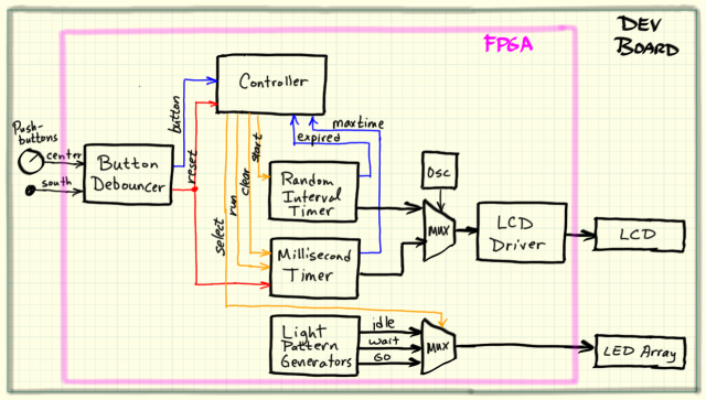
Major datapath elements include the millisecond timer, random interval timer, light pattern generator, display manager, and button handler for switch debouncing. The entire system to be designed resides within the magenta FPGA boundary; the development board hardware devices external to the FPGA are indicated, as well.
Step 3: Design the detailed operation of the datapath components
Each block of the datapath can be designed more or less independently of the others. For example, the millisecond counter design does not depend at all upon the design of the light stripe pattern generator. The following subsections detail the design of each of the datapath blocks.
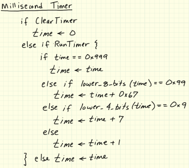
Millisecond Timer – Fundamentally a counter, the millisecond timer must be able to maintain, increment, and clear its value to zero, and increment at a one-millisecond rate. Primary inputs to the millisecond timer include the “Run Timer” and “Clear Timer” signals generated by the controller. When active, “Run Timer” allows the counter to increment, otherwise the counter maintains its present value. An active “Clear Timer” signal returns the stored count to zero. Note that the counter value must stop at “999” even when “Run Timer” is active.
A hexadecimal interface to the LCD already exists, saving considerable design effort on this project. However, simply connecting the counter to this interface shows a count sequence in hexadecimal format, clearly not useful for the final display. To solve this problem, the millisecond timer counter must occasionally increment by more than one to make the displayed value look correct. For example, consider the count as it begins from zero and approaches ten. In hexadecimal, this looks like 7, 8, 9, A, B, and so on. When the counter contains 9, adding 7 instead of 1 advances the count to 0x10 (“0x” denotes hexadecimal or base 16 notation) and looks correct for a standard decimal sequence. In a similar manner, adding 0x67 to a count of 0x99 produces a new count of 0x100.
As described in RTL Design for Data-Oriented Systems, register transfer statements express the behavior of a datapath element in text form. The following pair of diagrams shows the register transfer statements for the millisecond timer and the LabVIEW implementation of the millisecond timer; note that pacing the while-loop with a 1-ms wait yields the correct increment rate:
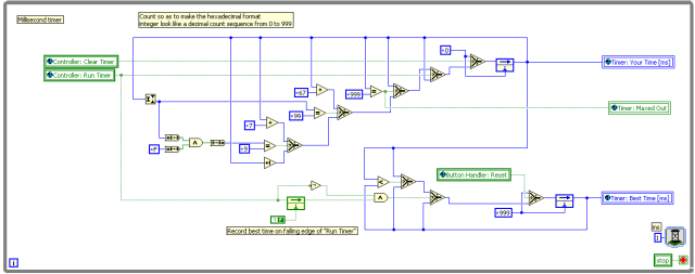
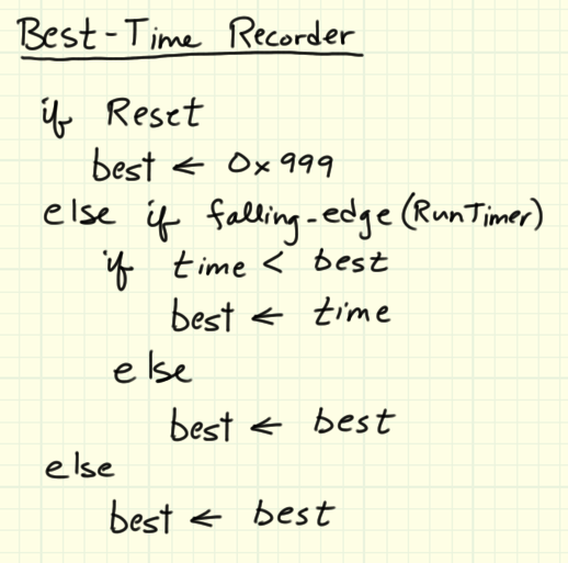
The LabVIEW block diagram for the millisecond timer includes a register to capture the best (shortest) reaction time of the day. This register initializes to 0x999 on power-up and also on an active “Reset” signal. A high-to-low transition on the “Run Timer” signal signifies the completion of a new time measurement, and this even enables comparison of the current best value with the new measurement and possible replacement of the current best value. The following diagram presents the register transfer statements for the best-time recorder:
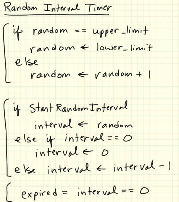
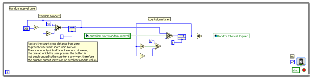
Random Interval Timer – The random interval timer (another counter) measures a time interval of roughly 3 to 10 seconds, with the specific interval length a random value that foils an attempt to guess when the time measurement will begin.
LabVIEW provides several random number generators, but these are not available within LabVIEW FPGA; it should be noted that LabVIEW FPGA provides a white-noise generator, but selecting this subVI introduces unnecessary complexity. Instead, a simple free-running 8-bit counter efficiently provides a random number between 0 and 255. Why? Because the pressed pushbutton event is completely unsynchronized with the counter value; sampling the free-running counter at the instant the pushbutton is pressed yields a nicely random value. The free-running 8-bit counter lower limit is constrained to one quarter of its maximum value establish a minimum wait time.
The random value initializes a down-counter when the control signal “Start Random Interval” activates. The down counter counts toward zero and remains at zero; a condition signal “Random Interval Expired” indicates to the controller that the random interval timer has reached zero.
The following pair of diagrams shows the register transfer statements and LabVIEW implementation of the random interval timer; note that pacing the while-loop with a 40-ms wait yields a random interval in the range of 2.52 to 10.2 seconds corresponding to the free-running up-counter values of 63 to 255 times 40 milliseconds:
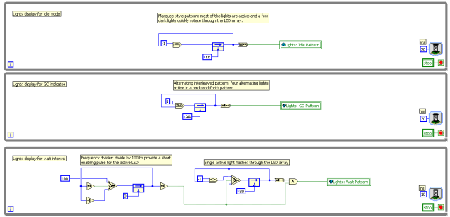
Light Stripe Display – Three distinct patterns must be applied to the light stripe. Each pattern is generated independently and in parallel with the others, and the controller operates a MUX to select the pattern that actually connects to the light stripe.
The “transparent FPGA” technique (see Rapid Development of Device Interfaces with a Transparent FPGA for details) greatly simplifies experimentation with LED patterns on the FPGA development board. A VI operating on the FPGA target connects the LED FPGA I/O nodes directly to a set of front-panel controls. This VI need only be compiled one time, a relatively lengthy process requiring several minutes compared to the essentially zero time required to compile a desktop VI. A desktop VI connects to the FPGA-targeted VI, and operates the LEDs by remote control, so to speak. The desktop VI executes instantly after any modification, thereby permitting new ideas to be tested quickly. Refer to the links section at the end of this article for the “Light Stripe Development” LabVIEW project.
After some experimentation, the following behaviors were adopted: the “idle mode” display implements a pattern reminiscent of an old-style movie marquee in which most of the lights are active and a few dark (off) lights quickly rotate through the LED array, the high-speed “GO!” pattern alternates four active lights active in a back-and-forth pattern, and the low-speed “wait” pattern rotates a single light through the array. A frequency divider reduces the on-time of the light so that it flashes only briefly in each position.
The LabVIEW implementation of each of these devices is illustrated below; note that each while-loop operates at a different rate:
The datapath contains enough detail at this point to warrant moving to the desktop prototype step.
Step 4: Design the controller state diagram
The five-step sequence contained in the “Reaction Timer Specifications” section above lays out the main flow of the controller state diagram:
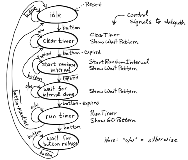
Many of the paths and transition conditions follow directly from the specifications, while others may seem less obvious. This diagram represents the results of several iterations of testing to get things right. The article State Machines for FPGA-Based Controllers describes how to implement the state diagram in LabVIEW.
IMPORTANT NOTE: Special care must be taken when working with multiple while-loop rates throughout the system. The system controller is paced at 1 millisecond to make it responsive at the same time resolution used by the millisecond timer. However, the random interval timer is paced at 40 milliseconds. Pulsing the “Start Random Interval” high for only one clock cycle not often catch the moment at which the random interval timer samples its control input. Therefore the controller activates “Start Random Interval” and then waits until “Random Interval Expired” goes inactive to indicate that the timer has begun its countdown. This type of signal “handshaking” enables systems that operate at different speeds to communicate correctly.
Step 5: Verify the design with a desktop prototype VI
In a traditional design flow based on HDLs (hardware description languages) such as VHDL and Verilog and digital circuit simulators such as Cadence NC-Sim and Mentor Graphics ModelSim, functional verification of the design requires development of a testbench to exercise the complete system in the simulator. A testbench is a special module that applies simulated inputs to the “unit under test” or UUT (the reaction timer system, in this case). The simulator generates the circuit response as tables of 1’s and 0’s or a set of waveforms to be interpreted by the designer. The iterative edit-simulate-revise debugging cycle proceeds much more quickly with a simulator rather than waiting to rebuild an FPGA bitstream file to test each new idea. After confirming that the system functions correctly, the designer can proceed to the hardware implementation step confident that few FPGA bitstream file rebuilds will be required.
LabVIEW provides the same type of testbench mechanism. However, creating the testbench VI (a separate VI from the “unit under test” VI) requires additional effort. For the purpose of this project and many others, simply building the reaction timer as a VI that runs on the desktop provides sufficient functional verification of the design to warrant committing to the FPGA-targeted version. Remember that the desktop prototype must be constructed using only those palettes that are available in the restricted palette set of LabVIEW FPGA.
Note that functional verification with a desktop VI sets LabVIEW apart from traditional design flows in several ways. First, the “design verification model” (DVM) VI can be tested incrementally as it is entered, and immediately upon completion. In contrast, the traditional flow requires additional effort to create a testbench. Second, the DVM VI provides a working model of the future FPGA-targeted system that can be easily appreciated and understood by others, including the client, providing an earlier opportunity for all to agree that the DVM satisfies the specifications or that the specifications should be modified. Third, the DVM VI’s emulation of future behavior on the FPGA-targeted system may in some cases reveal unexpected interactions among the subsystems more easily than by inspecting waveform plots.
The following video provides a brief tour of the desktop design verification model linked below as the “Desktop-Based Design Verification Model” LabVIEW project:
Step 6: Convert the desktop prototype to the FPGA target
The FPGA conversion process proceeds smoothly provided the desktop prototype was assembled with an eye toward the FPGA target. Major steps in this process include: create a new LabVIEW project, create a new FPGA target, add a VI to the FPGA target, copy-and-paste from the desktop prototype to the FPGA target, and add FPGA I/O. This last step (adding FPGA I/O) ranges from the trivial – changing a Boolean control to a pushbutton switch – to the complex, depending on the type of I/O. The reaction timer illustrates examples of each.
The following video briefly tours the completed reaction timer system as implemented on the FPGA target to provide context for the remainder of this section:
The previous section described most of the datapath construction; the remainder of this section describes those parts of the datapath added to the design verification model to create the FPGA implementation.
Button Handler – Pushbuttons and slide switches normally exhibit mechanical switch bounce or chatter. A single press of a pushbutton might liberate twenty or more transitions at the sub-millisecond level. A switch debouncer detects the initial transition and then filters out the subsequent transitions to present a single clean transition to the controller or datapath. This project includes debouncers on the “mushroom button” input and on the reset button. Note that the debouncers must reside in a single-cycle timed loop operating at 50 MHz to ensure the correct filtering time.
LCD Device Manager – The Xilinx Spartan-3E Starter Kit FPGA development board features the PowerTip PC1602-D Character LCD module (https://www.powertipusa.com/pdf/pc1602d.pdf), a 16x2 character liquid crystal display (LCD) operated by the Sitronix ST7066U Character LCD Controller (http://www.sitronix.com.tw/sitronix/product.nsf/Doc/ST7066U?OpenDocument). Chapter 5 of the user’s manual for Starter Kit board provides complete details for the interface and timing requirements of the LCD controller.
A device manager subVI and associated formatting subVIs provides a simple interface to the LCD. The “Manage LCD” subVI contains its own processing loop, and resides in its own space on the top-level VI. Companion subVIs including “Show Hex on LCD” and “Show Character on LCD” accept user-friendly inputs, format them into command messages, and push the messages onto a FIFO (first-in, first-out memory); the “Manage LCD” subVI pops messages from the FIFO and generates the required signal timing to pass the commands to the LCD controller.
In principle, the companion subVIs can connect anywhere that a standard LabVIEW indicator would be used, but two practical considerations motivate their placement in a single while-loop connected by global variables. First, transferring commands to the LCD takes some time: 48 microseconds for most commands, and up to 1,648 microseconds for the “Clear Display” and “Return Cursor Home” commands. A single call to the “Show Hex on LCD” subVI with U16 datatype generates 5 commands: a starting address and four ASCII characters, requiring a total of 240 microseconds. This time assumes that no other companion subVIs send messages to the FIFO. Each companion subVI locks the FIFO input to ensure that its message passes through the FIFO in the correct sequence, therefore the call to “Show Hex on LCD” could take longer than expected. Consequently, care must be exercised to ensure that the companion subVIs operate in loops that balance the needs of a responsive display and multiple users of the display.
Space requirements dictate the second consideration for the total number of companion subVIs in the design. Each appearance of a companion subVI on the block diagram requires its own chunk of space on the FPGA. Therefore, only one “Show Character on LCD” subVI is placed on the block diagram, and then called within a for-loop to create multiple messages to the LCD controller; this is the mechanism used to generate the text labels “time:”, “best:”, and “ms” around the numerical display.
The LCD-related VIs nicely illustrate how a designer may adopt different “design hats” in different areas of the datapath implementation. Most of the reaction timer design follows the traditional controller/datapath system model and RTL design techniques used by digital hardware engineers for decades, predating even HDLs and logic synthesis; the “digital hardware design hat” is firmly in place for the design of the millisecond timer, for example. On the other hand, effective use of the LCD subVIs requires more of a “software hat” or “LabVIEW G coding hat;” the for-loop structure embedded in a case-structure operated by the “First Call?” node certainly looks foreign when wearing the “RTL” hat. LabVIEW offers the designer a seamless transition between hardware-oriented and software-oriented design styles, facilitating their co-existence in the same design.
Step 7: Verify the design in hardware and refine as needed
Ideally the desktop DVM (design verification model) would flush out all design bugs, and the FPGA-targeted VI would operate as specified on the first build. Barring simple mistakes such as selecting the wrong FPGA pin when configuring an FPGA I/O node, the fact that the design operates in a fundamentally different target (the FPGA instead of a desktop computer) suggests that the FPGA-targeted design will operate differently, but hopefully with the desired functionality. For example, the switch debouncers are only necessary on the FPGA target. If they are not placed in a single-cycle timed loop, or worse yet, placed in a loop with a relatively long delay, then the FPGA-targeted design will likely operate erratically compared to its desktop ancestor. In other types of designs that must operate at or close to the FPGA development clock rate – VGA video is a good example – it is not practical for the desktop DVM to operate this quickly and with the needed waveform timing precision. Therefore, expect to experience a few re-compiles during this last stage of testing. Remember to revert back to the desktop DVM if the re-compiles seem to stem from basic functionality bugs.
The front-panel from the DVM serves as a diagnostic for the FPGA-targeted system. The front-panel indicators mirror the FPGA-based system’s controller state as well as its signal levels and register values. Detaching the USB cable breaks the connection to the front panel, of course, but does not disturb the FPGA system. Moreover, LabVIEW FPGA provides a mechanism to store the bitstream file in nonvolatile memory on the FPGA development board; with the correct jumper settings, the board will power up with the reaction timer system, eliminating the need for a desktop computer connection.
The LCD driver subVIs adds system complexity, require more FPGA resources, and increase the bitstream file build time. The following table compares two versions of the reaction timer -- one using the LCD on the Xilinx board, and the other using the LED on the NI board -- and also includes a "minimal design" that simply connects a pushbutton straight through to an LED:
| Resource | LCD Version | LED Version | "Minimal Design" |
|---|---|---|---|
| Total Slices | 23.1% (2151 out of 9312) | 15.1% (1410 out of 9312) | 3.2% (302 out of 9312) |
| Flip-Flops | 24.6% (2292 out of 9312) | 17.8% (1662 out of 9312) | 4.5% (416 out of 9312) |
| Total LUTs | 69.2% (3220 out fo 4656) | 43.3% (2018 out of 4656) | 8.0% (374 out of 4656) |
| Block RAMs | 0.0% | 0.0% | 0.0% |
| Build Time | 8 min 40 sec | 5 min 58 sec | 2 min 6 sec |
The "Minimal Design" column reveals the overhead associated with the LabVIEW FPGA interface through the USB cable. Also note the minimum build time of two minutes. The LED version has very little complexity between the timer register and the LEDs, therefore the resource consumption is primarily the reaction timer itself. The LCD therefore requires 8% more slices, 7% more flip-flops, and 26% more LUTs. The LED version build time requires 2.8 times that of the minimal design, and the LCD version requires 4.1 times that of the minimal design.
Refer to the first video in this article for a demonstration of the complete reaction system timer operating on the Xilinx Spartan-3E Starter Kit development board. The links section at the end of this article contains the complete LabVIEW projects that target both the Starter Kit board and the National Instruments Digital Electronics FPGA board. The latter version displays the reaction time in hundredths of seconds, and uses a pushbutton to temporarily display the best recorded time.
Conclusions
LabVIEW and the LabVIEW FPGA Module offer complete support for the entire system development process, from rapid prototyping of subsystem component behavior through system functional verification on the desktop and finally to testing and debugging of the final system. LabVIEW implements the traditional RTL style of digital hardware design, and offers LabVIEW G coding as a software-oriented approach that can be freely intermixed within the same design. The reaction timer design case study presented in this article illustrates how a capstone design project for a digital circuits and systems course can be implemented with LabVIEW.
