- Subscribe to RSS Feed
- Mark Topic as New
- Mark Topic as Read
- Float this Topic for Current User
- Bookmark
- Subscribe
- Mute
- Printer Friendly Page
myRIO sampling rate
Solved!10-23-2015 05:32 AM
- Mark as New
- Bookmark
- Subscribe
- Mute
- Subscribe to RSS Feed
- Permalink
- Report to a Moderator
I am new to myRIO and am using it to measure sine wave (0V to 5V) of from 10 Hz upto 20 KHz. I also need to do Fast Fourier Transform (FFT) of the measured signal in real time.
On the FPGA side of things, I am trying to keep things pretty simple, just read from 2 AI channels (Connector B: AI0 and AI1), therefore potentially able to read from each AI at 250 KS/s (as the device has a 500kS/s capability). Does this mean this program gets a data from two analog inputs exactly every 4 microsecond? If not, how do i ensure that the data is acquired at a fixed sampling rate?
I realised that we can add in FFT function in FPGA, but i wanted to manipulte the data acquired from Analog inputs before sending to FFT which i don't know how to do now. Can anyone explain me to how to do arithmetic data operation (muliplication, division and so) over the data acquired from Analog inputs and to reducde the resolution from 12 bits to 10 bits in FPGA program.
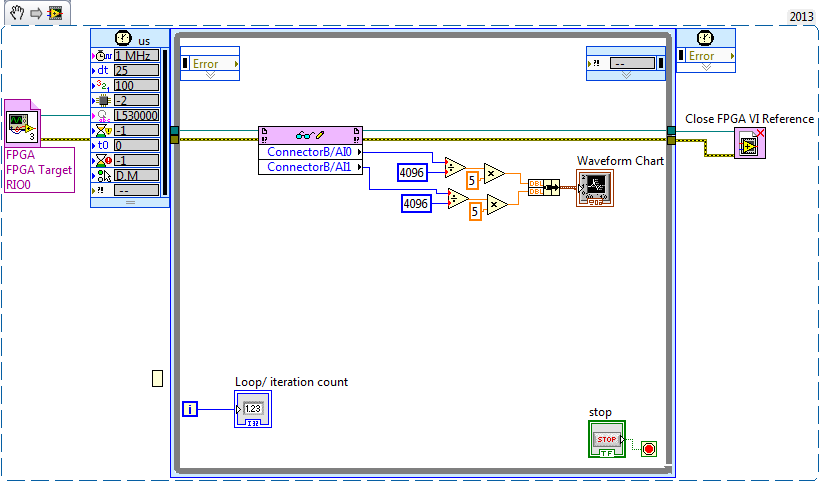
Later, i created a program in myRIO to read the 2 analog data from FPGA program that keeps running in a timed loop. In the myRIO program, the timed loop is configured to source type of 1 MHz clock with a time period of 25 microsecond.
Does this configuration mean the loop will run exactly every 25 microsecond?
When i configured the time period less than 10 micro second, myRIO stopped working. Why is that so?
Is it because that myRIO can't run as fast as FPGA?
Is it advisable to do the FFT of the analog data in myRIO side or FPGA side?
When i tried to do FFT using Power Spectrum in myRIO side, it asked for waveform data. What i acquire is analog data. How do i convert it into waveform data?
Though i read through forum for help, i couldn't get complete answer for my doubts
Forum threads i referred to:
Solved! Go to Solution.
10-24-2015
03:29 PM
- last edited on
01-04-2024
10:50 AM
by
![]() migration-bot
migration-bot
- Mark as New
- Bookmark
- Subscribe
- Mute
- Subscribe to RSS Feed
- Permalink
- Report to a Moderator
A lot of good questions here, I'll try to answer as many as I can as well as offer up a bit of advice.
First of all, if you are looking to acquire data at a very specific rate on the FPGA, you are going to want to use the Loop Timer VI. You are also going to want to use a DMA FIFO to transfer your data from FPGA to Real Time. Using a read/write node like you are currently doing means that you are going to either miss samples or read the same sample multiple times. The link below is a very good tutorial of how to do what I described above.
Later, i created a program in myRIO to read the 2 analog data from FPGA program that keeps running in a timed loop. In the myRIO program, the timed loop is configured to source type of 1 MHz clock with a time period of 25 microsecond.
Does this configuration mean the loop will run exactly every 25 microsecond?
When i configured the time period less than 10 micro second, myRIO stopped working. Why is that so?
Is it because that myRIO can't run as fast as FPGA?
In general, you should not run a timed loop much faster than 1kHz. Using the intenal timed loop nodes you can monitor the actual loop rate during runtime to see if f you are meeting your timing requirements.
The RT portion of your myRIO is slower than an FPGA in the sense that it cannot handle 40MHz loop rates (it makes up for this by being able to work with arrays much better) and it is important to remember that it is just a computer. The benefit of a real time operating system is that you have much greater control over the scheduler, not that it is faster (less jitter, not faster code). There is some more good reading below.
Is it advisable to do the FFT of the analog data in myRIO side or FPGA side?
When i tried to do FFT using Power Spectrum in myRIO side, it asked for waveform data. What i acquire is analog data. How do i convert it into waveform data?
I would say that it is generally advised to handle your FFT on the FPGA side as long as you have the resources available but for a lot of applications it probably doesn't matter in the end.
11-02-2015 08:45 AM - edited 11-02-2015 08:57 AM
- Mark as New
- Bookmark
- Subscribe
- Mute
- Subscribe to RSS Feed
- Permalink
- Report to a Moderator
Dear Matt J,
Many thanks for provding a detailed information.
I used a Loop timer VI (to acquire data in specific interval) in FPGA program and DMA FIFO ( to transfer data from FPGA to myRIO real time) and the program is working perfectly. I am doing the FFT on myRIO side now.
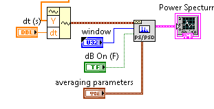
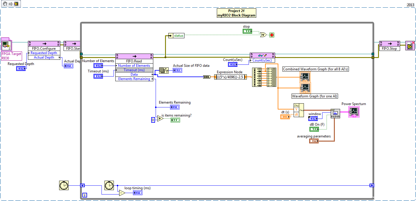
I am left with one additional question. Am using Power Spectrum FFT vi to perform FFT. For every loop in myRIO, am reading 1000 analog data points and sending it to Power Spectrum VI. Attached below the screenshot for reference.
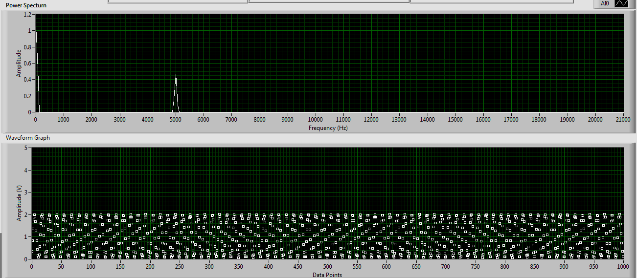
When i measured a sine wave (10Hz to 20 KHz) generated by Function Gen and read through analog input port, i am seeing an unwanted spike around 0 Hz.
E.g: Below is the screenshot captured when a sine wave of 5 KHz is measured. The spike is even bigger than the actual signal
There's no problem with Analog input portion as I am able to see a sine wave in waveform graph very clearly in real time.
Any idea what could be the possible reason and a possible fix?
As I doing a DC offset to the waveform generated, i can't fix the lower point of function gen voltage exactly to 0V.
I am afraid that could be one of the reaons causing a spike at 0 Hz
Thanks 🙂
12-14-2015 01:52 AM - edited 12-14-2015 02:21 AM
- Mark as New
- Bookmark
- Subscribe
- Mute
- Subscribe to RSS Feed
- Permalink
- Report to a Moderator
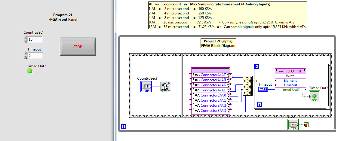
Though, i am able to measure signals upto 31.25 KHz from 8 AI's simultaneously (by using featurs such as using DMA FIFO and timer loop in FGPA @ 16 microsecond), i am facing a small issue.
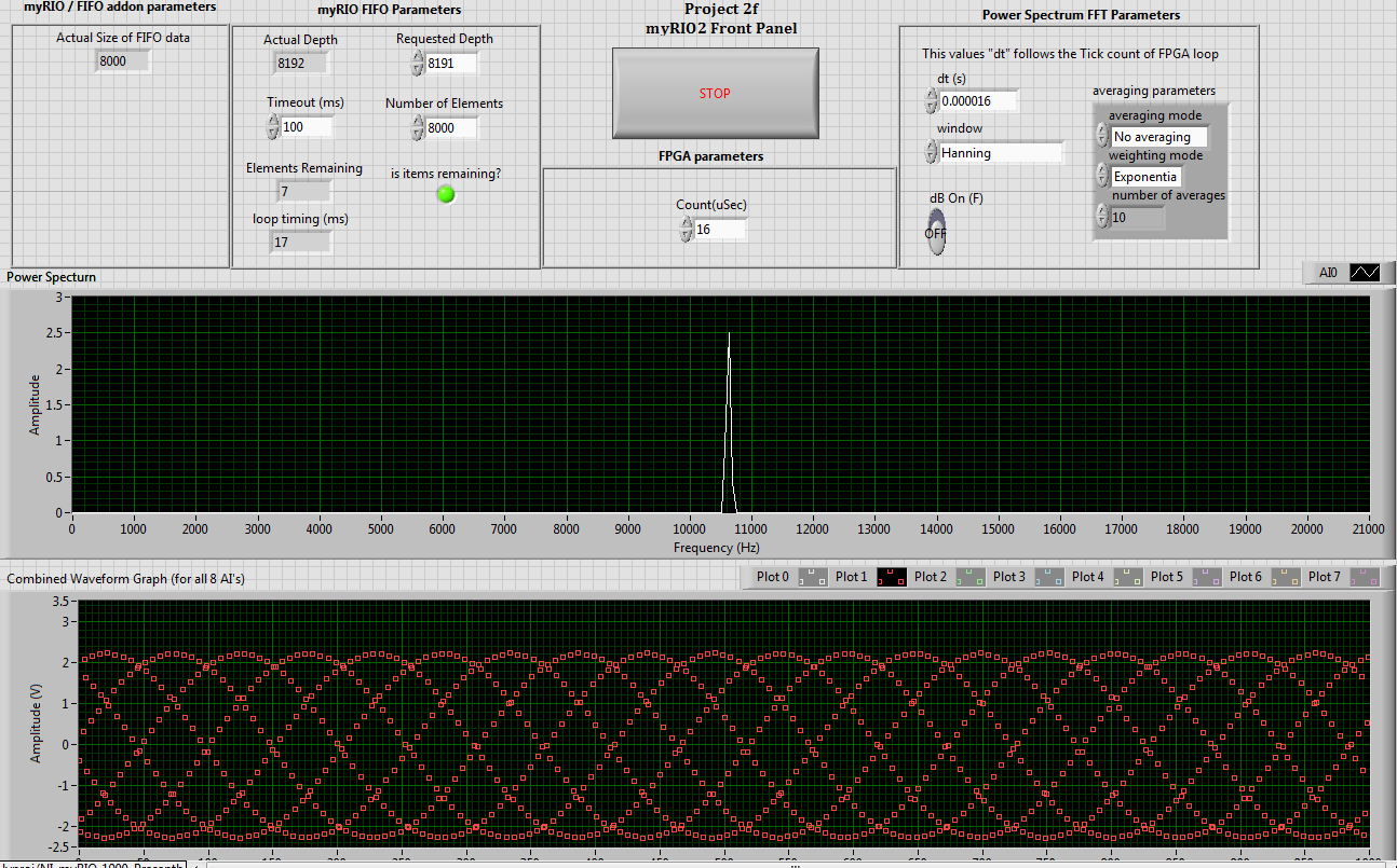
When i measure a 10 KHz sine wave from function generator, my power spectrum shows a spike around 10.6 KHz.
Should i add in any information in Power Spectrum or did I missed any steps?
"Screenshot of my Front Panel"
Screenshot of my Block Diagram
"Screenshot of my Block Diagram containing the Power Spectrum Portion"
Here, i chose
dt (s) = .000016
Window = Hanning
dB on = OFF
"Screenshot of FPGA Program"
12-14-2015 06:57 PM
- Mark as New
- Bookmark
- Subscribe
- Mute
- Subscribe to RSS Feed
- Permalink
- Report to a Moderator
Hi PrasanthTP,
Based on what you have done I can see that you have good understanding of communication between FPGA and Real Time targets. Just a few tips here that might help in solving the problems you are having:
When i measured a sine wave (10Hz to 20 KHz) generated by Function Gen and read through analog input port, i am seeing an unwanted spike around 0 Hz.
This is most probably caused by the DC offset from your function generator, as DC offset will appear as a peak at 0 Hz in the frequency spectrum.
Refer:
http://www.ni.com/white-paper/4278/en/
When i measure a 10 KHz sine wave from function generator, my power spectrum shows a spike around 10.6 KHz.
Assuming you are acquiring 8000 points of data everytime you try to read from DMA FIFO, you should make sure there is 8000 or more elements in the FIFO before reading from it. Reading 7000 elements and doing a FFT of 8000 elements is going to give peaks in the wrong frequencies. You might want to try this out:
VI Snippet (LabVIEW 2015): Ensuring elements inside DMA FIFO is more than the desired number of elements to read before reading them.
Also, try wiring a Zero constant the Timeout(ms) terminal to prevent DMA FIFOs from waiting in the loop. Instead, at the FPGA side, try to make sure there is no timeout occuring during the writing process to the DMA FIFO.
Hope this helps. ![]()
D.S Yiauw
National Instruments | ELP Engineer
CLAD
National Instruments | ELP Engineer
CLAD
12-14-2015 08:29 PM - edited 12-14-2015 08:33 PM
- Mark as New
- Bookmark
- Subscribe
- Mute
- Subscribe to RSS Feed
- Permalink
- Report to a Moderator
Dear D.S.Yiauw
Thanks for detailed explanation. I will implement your advise later today. The forum had been of great help from the very beginning
Meanwhile, i would like to throw some of my conceptual queries reg FPGA, RT and DMA FIFO
FPGA Portion
- How to make sure there is no timeout occuring during the writing process to the DMA FIFO in FPGA? Yet, maintaining a costant loop rate of 16 microsecond (i.e. a sampling rate of 62.5 KHz).
- What does the Requested number of elements (i assume, that means DMA size or FIFO size) do when we right click and configure the FIFO proprty under Project Explorer. In my case, i configured the value as 1023
RT Portion
- In FIFO configure node, the actual depth is shown as 8192
- What does this 8192 mean? Is it related to (1024 FIFO Size x 8 Channel = 8192 data elements)
- In FIFO read node, i am acquiring 8000 elements everytime when I read from DMA FIFO
- Is there a relation between Depth vs No of elements I read?
- As my depth size is shown as 8192, should I read all the 8192 elements from FIFO at one shot to ensure that i don't miss any elements?
Can anyone give me an example that will allow me to visualise how data is tranferred from FPGA to RT via DMA FIFO and what each parameter (DMA size, depth, no of elements to read, time out) play a role ?
12-15-2015 12:07 AM
- Mark as New
- Bookmark
- Subscribe
- Mute
- Subscribe to RSS Feed
- Permalink
- Report to a Moderator
Hi PrasanthTP,
I'm glad that I'm able to help. I might not be able to answer all your questions precisely but I'll try my best.
FPGA Portion
How to make sure there is no timeout occuring during the writing process to the DMA FIFO in FPGA? Yet, maintaining a constant loop rate of 16 microsecond (i.e. a sampling rate of 62.5 KHz).
Timeout occurs when you are trying to write new data into a full-buffered FIFO, or read data from an empty FIFO. To prevent timeout from occuring, try to read from FIFO with rate fast enough to prevent the FIFO from overflowing. I've done a little bit of calculation based on your application to know if your FIFO is overflowing:
Writing to FIFO:
62500 Hz x 8 channels = 500000 Data into FIFO in 1 second
Reading from FIFO:
8000 elements / 0.017 second = 470588 Data from FIFO in 1 second
Where 0.017 second is your FIFO reading loop time based on your timing benchmark, which in this case, your FIFO is most probably overflowing, so some of your data might be lost during acquisition. The way you are acquiring data at a constant loop rate is correct, you just have to increase the speed of your FIFO reading from the host side.
What does the Requested number of elements (i assume, that means DMA size or FIFO size) do when we right click and configure the FIFO proprty under Project Explorer. In my case, i configured the value as 1023
The requested number of elements option when we configure DMA/FIFO is the size of the buffer for the DMA/FIFO. Usually leaving the default value as it is will be sufficient as long as the rate of reading from the DMA/FIFO is fast enough to prevent overflowing.
RT Portion
- In FIFO configure node, the actual depth is shown as 8192
- What does this 8192 mean? Is it related to (1024 FIFO Size x 8 Channel = 8192 data elements)
- In FIFO read node, i am acquiring 8000 elements everytime when I read from DMA FIFO
- Is there a relation between Depth vs No of elements I read?
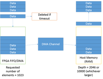
For these two questions, I'll summarize the info from the link below into this: The depth of FIFO configured in RT host is the buffer size allocated in the RT host's RAM for the FIFO. Normally the depth is set to double the size of the FIFO set in the FPGA side or 10000 elements, whichever is larger.
For the flow of data from FPGA to RT via DMA FIFO, please refer to the image below:
In the image above, data is writen to FPGA DMA FIFO, which has a size of 1023 elements. The data is sent to the RT host's memory directly through the DMA channel, without going through the RT processor. The depth of the buffer allocated for the DMA FIFO at the RT side is 10000 elements, as LabVIEW automatically coerces to the larger value between twice the FPGA DMA FIFO size or 10000 elements. Data is then read out from the RT host VI. If the writing rate at the FPGA side is faster than reading rate of the RT host side, eventually overflowing will occur at the FPGA DMA FIFO, and new elements will not be writen to the DMA FIFO and will be lost.
Hope this helps.
D.S Yiauw
National Instruments | ELP Engineer
CLAD
Reference:
http://digital.ni.com/public.nsf/allkb/1B7F7C2C9A650DE186257B6E003FDED4
http://zone.ni.com/reference/en-XX/help/371599H-01/lvfpga/fifo_write/
National Instruments | ELP Engineer
CLAD
01-18-2016 03:04 AM - edited 01-18-2016 03:05 AM
- Mark as New
- Bookmark
- Subscribe
- Mute
- Subscribe to RSS Feed
- Permalink
- Report to a Moderator
Thank you very much for detailed explanation. I got whole new level of understanding on the FIFO portion.
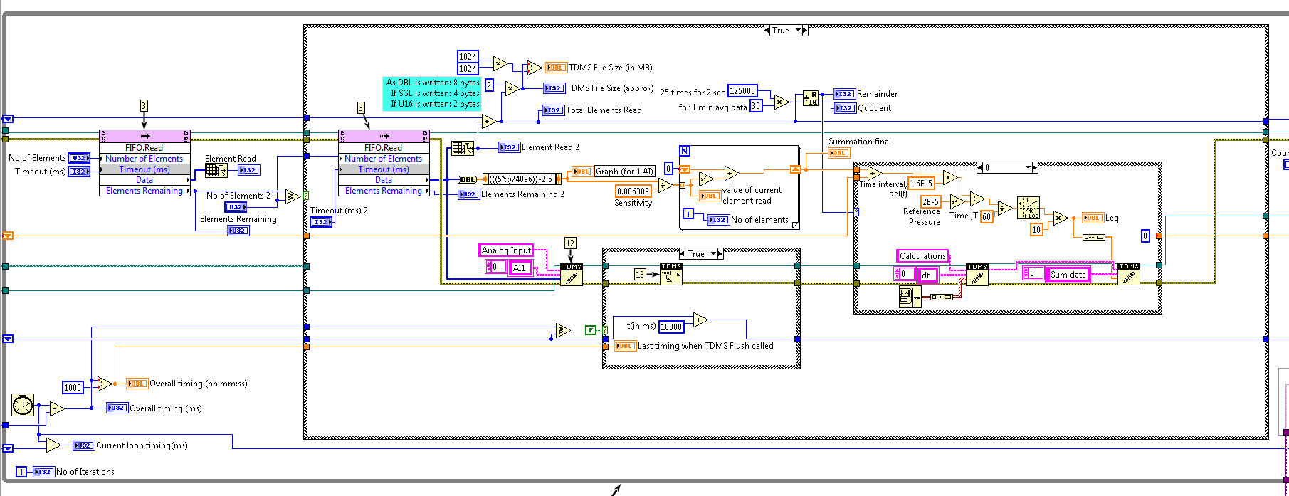
I am trying to acquire 625000 samples/ sec from FPGA via FIFO to myRIO. Then, I want to have sum of every 2 minutes of acquired analog data to perform further operation and log the data into TDMS.
In addition, i want to perform Fast Fourier Transform on every 0.5 second chunk of data (31250 samples) and store it in TDMS file concurrently.
ON FGPA side
i managed to read data from 1 Analog Input at 62.5 KHz (16 microsecond). Then, I write the data into FIFO.
On myRIO side,
- Reading 5000 data from FIFO for evry loop(whenever it gets 5000 or more elements). I assigned the FIFO's depth size as 10124
- Logging the raw data into a TDMS file (just for testing purpose, not imporant)
- Doing some basic mathematical operation on these 5000 elements and sum those 5000 elements and store it in shift register so that i can access in next loop
- I do this as I want to calculate the sum of analog input for every 1 min or 2 min so that I can perform some operation over it
- I keep adding these 5000 elements and add it to the previous sum until it becomes sum of analog input acquired for 2 mins.
- Then, i perform some operation and data is logged into TDMS file, but in different group
The doubts and uncertainities I have are
- Is there an efficient way to implement summation of 1 mins of data (625000 elements/ sec * 60 sec/ min)
- Is it possible to do this entire summation for 1 min chunk of data in FGPA portion? If so, can anyonne share some reference materials?
- I need to perform FFT on every .5 second data (i.e. 31250 elements). Is it better to implement it in FPGA or myRIO and why? Can you advise me on some good reference materials on FFT?
FPGA screenshot
myRIO - Block Diagram Screenshot
myRIO Front Panel - Screenshot

01-21-2016 04:21 AM
- Mark as New
- Bookmark
- Subscribe
- Mute
- Subscribe to RSS Feed
- Permalink
- Report to a Moderator
Hi there this section seems to be exactly waht I need with regards to setting a specific rate however the link:
http://www.ni.com/tutorial/4534/en/
sends me to an error.
Do you by any chance know how I could find it?
Thank you
07-08-2016 03:01 PM
- Mark as New
- Bookmark
- Subscribe
- Mute
- Subscribe to RSS Feed
- Permalink
- Report to a Moderator
Hello friend,
Your program helped me a lot to do the mine. You resolved me some doubts I had. Now, I have a question, and I hope you can help me. I am doing a "standalone" (witout the PC) application that acquire data of an analog port, and I need save the data in a USB or in the myRIO.
Right now I can run the FPGA VI like a "standalone" application and the VI of myRIO too, but the data don't save. Can you help me?, someone can help me?.
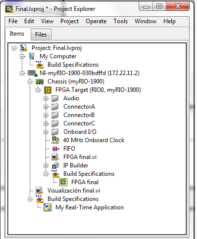
I built the FPGA VI and the VI of myRIO and created the specifications for both of them run like a standalone application, that is working.
Here I have the FPGA VI, I acquire data of AI1 port and use a FIFO to read and write the data between the FPGA and myRIO. I use the button and the led 0 and 3 of the card for indicate that the application is working.
And here the main VI. I read the data like you and next I save and use the FFT. For that, I used the buttom of the card to activated the save. This work too.
My problem is that, the data don't save with the standalone application, while I use the USB conexión and run my program, it work perfectly, indicate when is saving and the data is almacened, but with the standalone application the data don't be save, like if the FIFO doesn't work.
Do you have any idea? or someone?.
Thanks, excuse my bad english. I hope that you can understand me.

