- Subscribe to RSS Feed
- Mark Topic as New
- Mark Topic as Read
- Float this Topic for Current User
- Bookmark
- Subscribe
- Mute
- Printer Friendly Page
Design Guide to Power Electronics Co-Simulation with Multisim and LabVIEW
11-03-2011 10:39 AM
- Mark as New
- Bookmark
- Subscribe
- Mute
- Subscribe to RSS Feed
- Permalink
- Report to a Moderator
The software installers and latest code for this design guide are available for download.
This is a guide to power electronics demonstration samples for Multisim/LabVIEW co-simulation. These new tools are intended to enable desktop development of power electronics control IP for LabVIEW FPGA, enabling you to develop/test/debug/validate before you compile to physical hardware.
By exploring these samples, you can learn basic features of the co-simulation environment as well as the techniques you will need to accurately simulate LabVIEW FPGA control systems with your power electronics circuits. By exploring the samples and suggested exercises in this document with live interactive LabVIEW front panels, you can also enhance your intuitive understanding of the switch mode power electronics circuits and control systems.
The goal of these graphical system design tools is to significantly accelerate the development of inverter control systems, by enabling you to develop your exact deployment code on the desktop (without long FPGA compiles), and using formal software verification techniques (build each IP block to specification and perform functional verification testing on the desktop whenever changes or updates are made).
NI hopes the new tools will serve as a catalyst and platform for innovation and creativity and would like to invite you to expand and enhance the samples contained in this guide. We encourage you to develop, document and share through the online Power Electronics Development Center community site the following: 1. Power electronics circuit examples, 2. Power electronics control algorithms for LabVIEW FPGA, 3. Multisim power electronics component models, 4. Comparisons between physical test data and simulation results, and 5. Training materials or curriculum for industry professionals or university students.
Design guide goals
- Enable hands on learning for fundamentals of co-simulation
- Enable hands on learning for power electronics control with LV FPGA/RT
- Enable hands on learning for switch mode power supply circuit design
Design guide roadmap
- Provide examples that start with simple/basic control schemes (like voltage over frequency control of an inverter) and take the student step up to advanced control schemes (like space vector control, active power factor correction)
- Organize all of the LabVIEW FPGA IP cores into a single organized subfolder.
- Provide help documentation and testbench applications for all IP cores. The testbench apps are used to test/verify correct functionality of the individual IP core. They also provide a great way to learn how each IP core is implemented- for example, let me see how the slew rate limit on the PWM IP core works?
- Move the LabVIEW FPGA IP cores to an open source online collaborative project. Ownership should be taken over by the developer community- a mix of researchers in industry and academia.
- Move the design guide to an online wiki style forum. Ownership should be taken over by the developer community.
11-04-2011 11:01 AM
- Mark as New
- Bookmark
- Subscribe
- Mute
- Subscribe to RSS Feed
- Permalink
- Report to a Moderator
There is a mistake in the instructions for how to calculate the phase delay on the 3-phase inverter output filter (pages 70-72 of the design guide). . . If anyone has time to fix it, please post your update and attach the updated Multisim schematic. I haven't found time to look at it yet but I think you will probably need to put three sinusioidal sources with 120, 240 degree phase offsets on each line of the inverter at the output of the transistors (Va, Vb, Vc), and do the Single frequency AC analysis slightly differently to calculate the correct phase shift.
Background:
I ran the output filter phase calculation for 50 Hz and didn't get the right result... Recently the inverter wall demo was updated for events in Europe-- operating on 240 VAC and 50 Hz. This requires a few changes to the code: 1. The RMS calculator should use 1000 samples/frame for a 50 Hz cycle (0.02 s), rather than 833 samples/frame for 60 Hz. 2. The PLL reference frequency should be changed to 50 Hz- this is optional since 50 Hz is within the min/max range as it was configured, 3. The output filter phase offset should be updated for the correct amount of phase shift for the RLC at 50 Hz, 4. The demo actually operates on single phase power so the FPGA code includes delay blocks that shift Phase A to produce simulated waveforms for phases B, C with the appropriate phase offsets-- so these delay blocks must be updated to have the correct offsets for 50 Hz power (for 50 Hz, configure the Discrete Delay block for a Phase B delay of 333 FPGA clock ticks (40 MHz clock), rather than 278 FPGA clock ticks for 60 Hz).
Note: Like most of the samples in the design guide, this inverter wall proof of concept is intended to be a simple example for training purposes and doesn't represent the control system structure you would want to use for a commercial deployment. For that, consider using either a stationary reference, natural reference, or a synchronous rotating reference frame control scheme, known as dq control. In this last case, the grid current and voltage waveforms are transformed into a dq reference frame that rotates synchronously with the three phase grid voltage. The angle calculation from the PLL is fed into Inverse Clarke, Park transforms, etc. and the dq currents and voltages are used by the control loops. These schemes enables the active and reactive power to be controlled independently. You can find Park/Clarke transform IP blocks in the power electronics IP library for LabVIEW FPGA (included with NI SoftMotion 2011 f1) or on the LabVIEW FPGA IP net space vector examples here.
Speaking of that... Would anyone be interested in adding examples to the 3-phase inverter part of the design guide for stationary, natural, and/or synchronous rotating reference frame control schemes? It would be great to be able to compare the pros/cons of the different control schemes used in industry.
11-07-2011 12:13 PM
- Mark as New
- Bookmark
- Subscribe
- Mute
- Subscribe to RSS Feed
- Permalink
- Report to a Moderator
Someone asked about how to write LabVIEW FPGA code so it can be tested in the desktop co-simulation environment or in a simple test-bench application for validation. I updated the section of the "Brushed DC Motor H-Bridge (Basic)" section of the co-simulation guide to add a link. Chapter three of the CompactRIO Developer Guide has a section on writing modular, reusable subVIs and test them using simulation (page 162).
There are a number of features built into LabVIEW FPGA to enable this, such as conditional compile which enables you, for example, to use one clock source for desktop simulation and the actual FPGA clock when deployed.
I have a slide presentation and training material on the same topic that I'd be happy to post if anyone is interested.
12-01-2011 10:36 AM
- Mark as New
- Bookmark
- Subscribe
- Mute
- Subscribe to RSS Feed
- Permalink
- Report to a Moderator
I'll update the Multisim schematic in the design guide later, but in the mean time you can find LabVIEW code to properly calculate the output filter phase offset in the new three-phase inverter reference design.
12-07-2011 07:38 AM
- Mark as New
- Bookmark
- Subscribe
- Mute
- Subscribe to RSS Feed
- Permalink
- Report to a Moderator
I thought I would pass on a performance tip for co-simulation with Multisim. Co-simulation makes good use of multi-core machines and you will see significant performance improvements on a multi-core machine. My rule of thumb would be:
Minimum number of cores = (Number of cores for LabVIEW based on LabVIEW diagram) + (Number of Multisim Design blocks on LabVIEW diagram) + (1 spare core)
For example, on the simple design below, I suggest 3 cores (1 + 1 + 1).
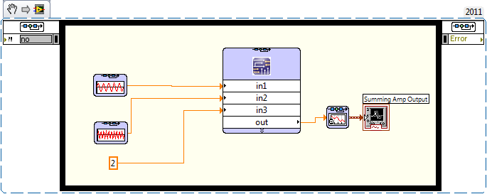
If you add one more Multisim Design block, I suggest 4 cores (1 + 2 + 1).

Senior Software Developer
National Instruments
Circuit Design Community and Blog
If someone helped you, let them know. Mark as solved or give a kudo. 🙂
11-04-2012 05:27 AM
- Mark as New
- Bookmark
- Subscribe
- Mute
- Subscribe to RSS Feed
- Permalink
- Report to a Moderator
Hi, I've got a multi-core machine, do I need to assign the cores to each of the tasks if I want to improve the co-simulation performance?
11-05-2012 07:39 PM
- Mark as New
- Bookmark
- Subscribe
- Mute
- Subscribe to RSS Feed
- Permalink
- Report to a Moderator
You don't need to manually assign any processor cores. The co-simulation tools automatically take advantage of multiple cores.
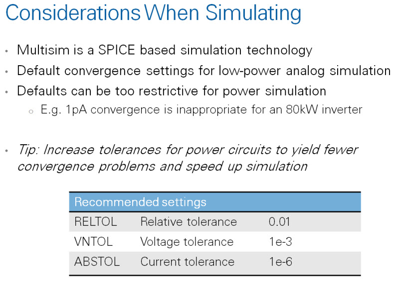
Also, make sure your simulation error tolerances in Multisim are appropriate for simulating switched mode power electronics. The default settings are for small signal analysis rather than switching power converters.
You can download the entire slide deck from NIWeek 2012 here:
Introduction to Power Electronics Design with LabVIEW FPGA and NI Multisim Co-Simulation
08-03-2014 03:49 PM
- Mark as New
- Bookmark
- Subscribe
- Mute
- Subscribe to RSS Feed
- Permalink
- Report to a Moderator
Hi there! Is there anyone working on islanding detection of grid-connected inverter using the co-simulation? I will appreciate an insight! Thanks.
