- Document History
- Subscribe to RSS Feed
- Mark as New
- Mark as Read
- Bookmark
- Subscribe
- Printer Friendly Page
- Report to a Moderator
- Subscribe to RSS Feed
- Mark as New
- Mark as Read
- Bookmark
- Subscribe
- Printer Friendly Page
- Report to a Moderator
myDAQ mini-lab: Op Amp III -- Voltage follower
Course Linkage: Linear Circuit Analysis >> Operational Amplifiers >> Voltage Follower
Measurement Techniques: ELVISmx DMM (voltmeter and ammeter)
<hr width=”75%”>
Introduction
Overview: Electronic systems combine smaller interconnected subsystems, often with voltage signals conveying information from one subsystem to the next. Interconnecting subsystems together without regard for loading effects can lead to unexpected reductions in the signal voltage. The voltage follower, perhaps the simplest op amp circuit possible (an op amp and a single wire), serves as a “buffer” between two subsystems. The voltage follower replicates the source system’s output voltage without loading and drives the input of the destination subsystem with sufficient current to maintain the necessary signal voltage.
Objectives: In this mini-lab you will:
- Measure the output voltage of a potentiometer-based voltage signal source under no-load and loaded conditions
- Measure the current drawn from the voltage signal source under no-load and loaded conditions
- Insert a voltage follower and investigate the improved ability of the signal source to communicate its voltage signal to the load
Demonstration: The following video illustrates the problem that loading effects can cause when two subsystems connect directly together:
Equipment
- NI myDAQ
- Breadboard
- Connecting wire
- Alligator clip test leads
- Texas Instruments (TI) TL072 op amp or similar device
- Resistors, ¼-W 5% carbon film: 1.0K (two), 2.2K (two), 10K
- 10K potentiometer
- LEDs (light emitting diodes) (two)
NOTE: Any dual-supply op amp is suitable for this project. Be sure to use the correct pin numbers, though, because these vary from one device to the next. Refer to the data sheet for your device (search www.datasheetcatalog.com) or ask your instructor for assistance.
Deliverables
- Submit your work in the form of a homework set problem or lab notebook entry according to the requirements of your instructor
- Submit your work for each underlined boldface item, and clearly label the item with its section letter and task number
A. Experience the loading effect problem by measurement
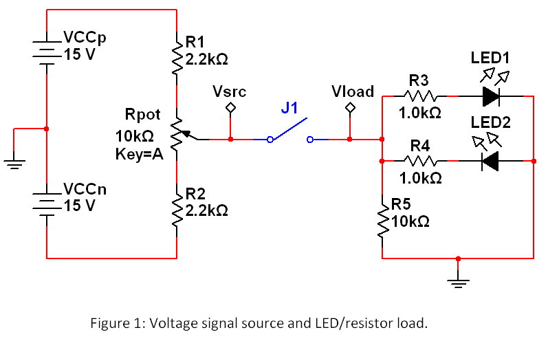
- Draw the circuit of Figure 1, a voltage signal source based on a potentiometer connected via a switch to a load consisting of resistors and LEDs:
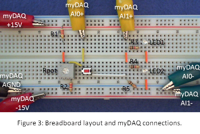
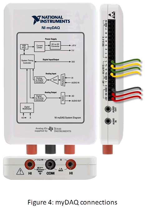
- Construct the circuit of Figure 2 with myDAQ and a breadboard; see Figure 3 for the recommended layout and Figure 4 for the myDAQ connections. NOTE: Leave room as shown in Figure 3 for the op amp voltage follower to be added later.
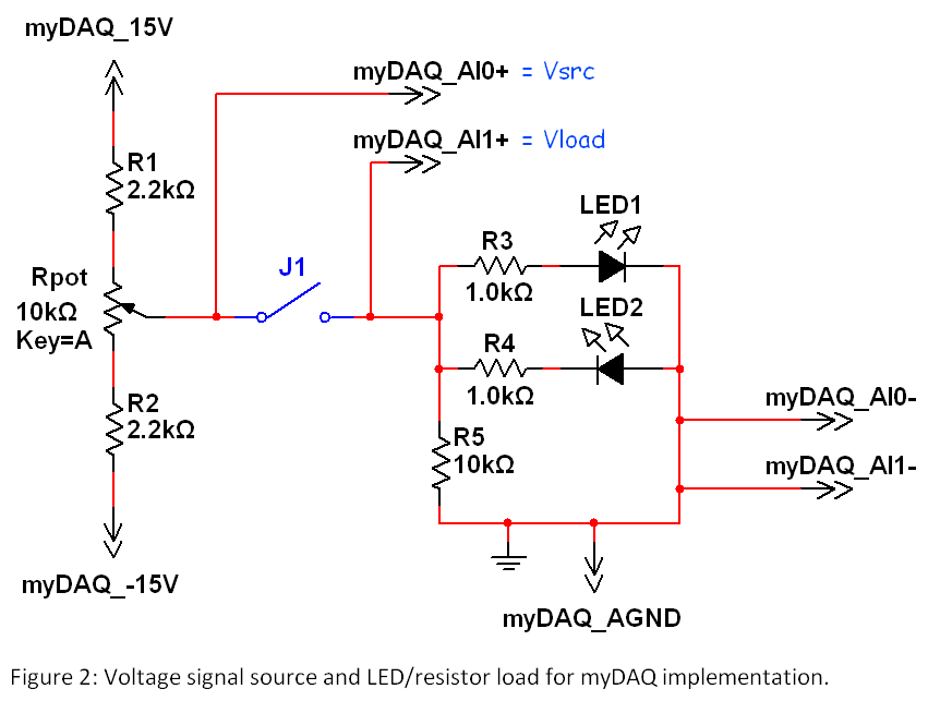
- Download and run “Show AI Voltage.vi” linked at the bottom of this document. Use this VI to measure the analog voltage inputs AI0 (Vsrc) and AI1 (Vload). Set the "digits" (digits of precision to display) control to 1.
- Adjust the potentiometer dial and ensure that the AI0 indicator varies throughout the -10V to +10V range.
- With the switch open (“no-load” condition), adjust the potentiometer to set the signal source voltage Vsrc to -10.0V as displayed for AI0 on “Show AI Voltage.” Close the switch to connect the LED load (“loaded” condition); measure and record the signal load voltage Vload.
- Repeat Step 5 in two-volt steps from -10.0V to +10.0V, i.e., -10.0V, -8.0V, -6.0V, and so on.
- Create a data table to present your measurements for no-load Vsrc and loaded Vload.
- Ideally the signal source voltage should reach the load unchanged. According to your measurements, report the maximum voltage error between the intended signal source voltage and the actual load voltage.
- While pressing the switch, adjust the potentiometer dial until LED1 just barely lights. Measure and record this value of Vload required to activate the LED.
- Release the switch, and adjust the potentiometer dial to make Vsrc match the value you recorded for Vload in the previous step.
- Close the switch. Respond: Does the LED still light?
The next video shows some expected results for this section.
B. Learn the underlying principles
The following video tutorial discusses why excessive loading of a high-resistance voltage signal source causes substantial reduction in the intended voltage signal level. The voltage follower, a simple circuit based on an op amp, is presented as a circuit that replicates the source voltage signal with no loading effects to drive the load with the intended signal level:
C. Connect the principles to your measurements:
- Insert the ELVISx DMM ammeter between the signal source and load as shown in Figure 5; Figures 6 and 7 show the recommended breadboard layout and myDAQ connections:

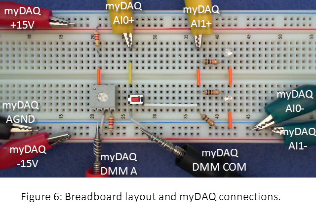

- Use DMM probe clips if you have them available, or coil a wire around the probe tip with one end of the wire long enough to connect into the breadboard.
TIP: Wrap the wire around the probe tip to form a coil, remove the coil and bend it slightly, and place it back on the coil (bending the coil ensures a snug fit):
- With the switch open (“no-load” condition), adjust the potentiometer to set the signal source voltage Vsrc to -10.0V as displayed for AI0 on “Show AI Voltage.” Measure and record the current that leaves the signal source Isrc. Close the switch to connect the LED load (“loaded” condition); measure and record the signal source current Isrc.
- Repeat Step 2 in two-volt steps from -10.0V to +10.0V.
- Create a data table to present your measurements of Vsrc (no-load), Isrc (no-load) and Isrc (loaded).
- Remove the switch.
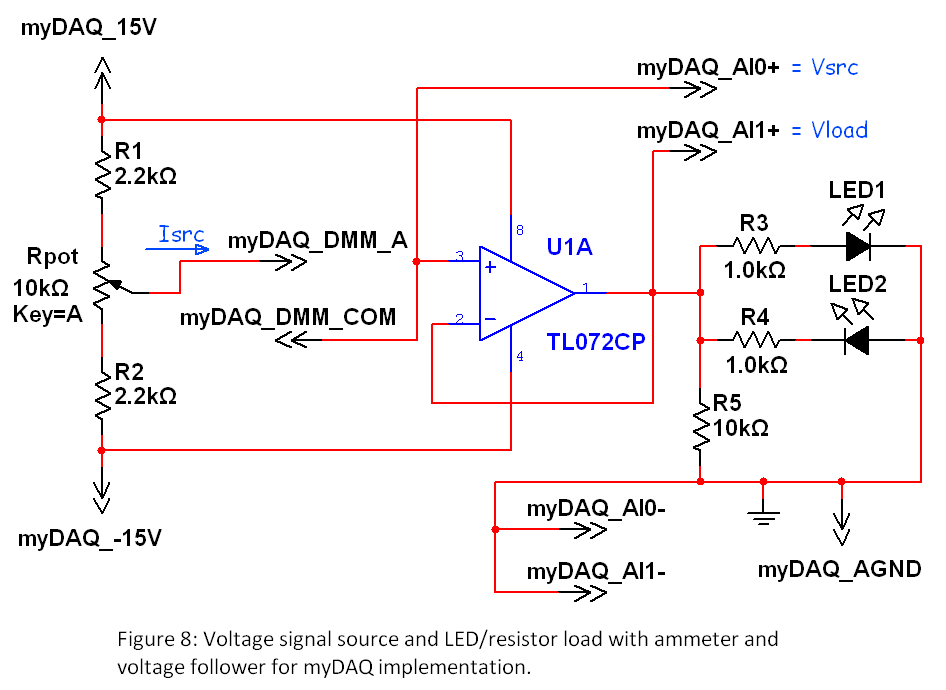
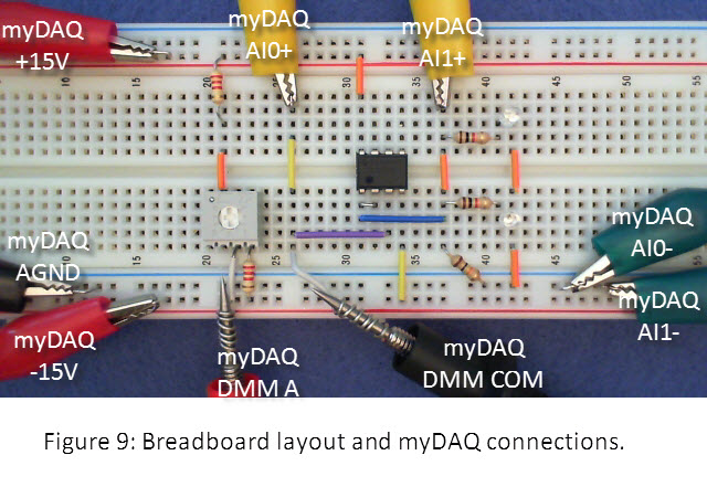
- Insert the voltage follower between the signal source and the load as shown in Figure 8; Figure 9 shows the recommended breadboard layout and myDAQ connections:
- Step the value of Vsrc from -10.0V to +10.0V as before and collect measured values for Vsrc, Vload, and Isrc.
- Create a data table to present your measurements of Vsrc, Vload, and Isrc.
- Ideally the signal source voltage should reach the load unchanged. According to your measurements, report the maximum voltage error between the intended signal source voltage and the actual load voltage.
D. Build your intuition:
- Respond: Where does the op amp get the current necessary to support the load voltage at the required level?
- Respond: Explain why does the voltage follower not load the signal source.
For more information
