FPGA Derived Clock Rate Calculator using LabVIEW
- Subscribe to RSS Feed
- Mark as New
- Mark as Read
- Bookmark
- Subscribe
- Printer Friendly Page
- Report to a Moderator
Products and Environment
This section reflects the products and operating system used to create the example.To download NI software, including the products shown below, visit ni.com/downloads.
- LabVIEW
Software
Code and Documents
Attachment
Overview
This VI demonstrates how to calculate the derived clock rate and the number of ticks per iteration for a desired clock rate.
Description
Creating a FPGA derived clock allows to generate custom update rates for applications. If the desired clock rate is below the range of the FPGA derived clock (<2.5 MHz), it is possible to generate a derived clock with a higher frequency. Using a Single Cycle Timed Loop (SCTL) with empty iterations is one possiblity to achieve the desired rate.
One example for achieving the CD sample rate of 44.1 kHz, a derived clock rate of 47.407 MHz (32/27 * 40 MHz) can be used and with executing each 1075th iteration of a SCTL, which gives you 44.0999 kHz. One alternative solution is configuring the "Wait" function and waiting the number of ticks.
The VI calculates all possible FPGA derived clock rates returns the best fitting rate of the derived clock with the number of ticks to wait and the occuring error of the clockrate.
Note that at the low end of the derived clock (2.5 - 5 MHz) not all combinations of the derived clock are possible. You need to test it in the actual FPGA Derived Clock dialog to verify.
Requirements
Software
- LabVIEW Base Development System 2012 (or compatible)
Hardware
- No hardware is necessary to use this example VI
Steps to Implement or Execute Code
- Run the VI
Additional Information or References


**The code for this example has been edited to meet the new Community Example Style Guidelines. The edited copy is marked with the text ‘NIVerified’. Read here for more information about the new Example Guidelines and Community Platform.**
Example code from the Example Code Exchange in the NI Community is licensed with the MIT license.
- Mark as Read
- Mark as New
- Bookmark
- Permalink
- Report to a Moderator
I modified the array that went into the last FOR loop so it didn't just take the top 20 answers (removed array subset). Instead, I left them all and found a combination that works with my Virtex-V. None of the first 20 had worked... but #32, a 9/10, ratio did give me something that could be divided down to 750 kHz.
A more complete program would ask for the FPGA used and weed out derived frequencies that are invalid using Virtex-5 FPGA User Guide (p.58) & Virtex-5 DC and Switching Characteristics Data Sheet (p.57) for the Virtex-V. See discussion by Donovan B in "derived clock problem? "
- Mark as Read
- Mark as New
- Bookmark
- Permalink
- Report to a Moderator
Thank you for providing this. This is a quick and dirty way of getting the needed clock.
Engineering - The art of applied creativity ~Theo Sutton
- Mark as Read
- Mark as New
- Bookmark
- Permalink
- Report to a Moderator
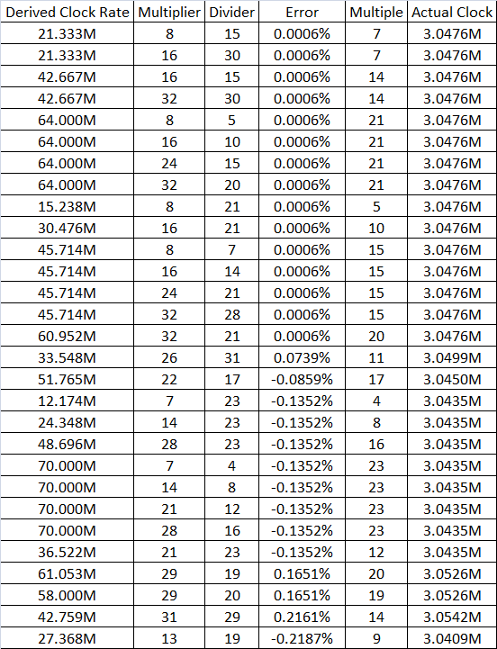
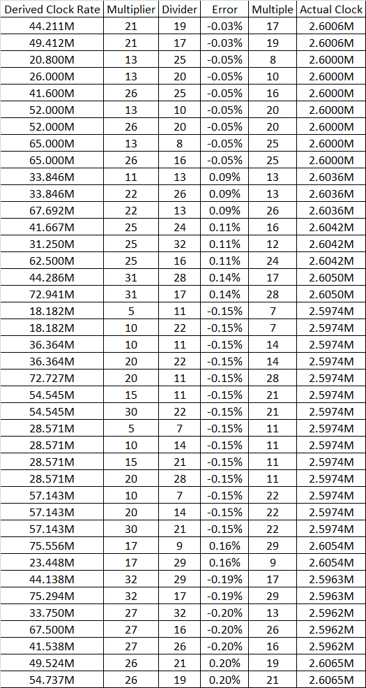
Sorry for the question but it is my first contact with such kind of technlogy.
May I obtain the following values obtained from calculator with PXI-785xr?:
2.1296MHz
2.6013MHz
3.0476MHz
- Mark as Read
- Mark as New
- Bookmark
- Permalink
- Report to a Moderator
Assumed maximum derived clock rate: 80 MHz
Not all options may work, but they are ordered from closest to farthest.
- Mark as Read
- Mark as New
- Bookmark
- Permalink
- Report to a Moderator
2.6006MHz
- Mark as Read
- Mark as New
- Bookmark
- Permalink
- Report to a Moderator
3047600Hz. Same assumptions as above. Anybody know how to attach csv files to a reply?