- Document History
- Subscribe to RSS Feed
- Mark as New
- Mark as Read
- Bookmark
- Subscribe
- Printer Friendly Page
- Report to a Moderator
- Subscribe to RSS Feed
- Mark as New
- Mark as Read
- Bookmark
- Subscribe
- Printer Friendly Page
- Report to a Moderator
Description:
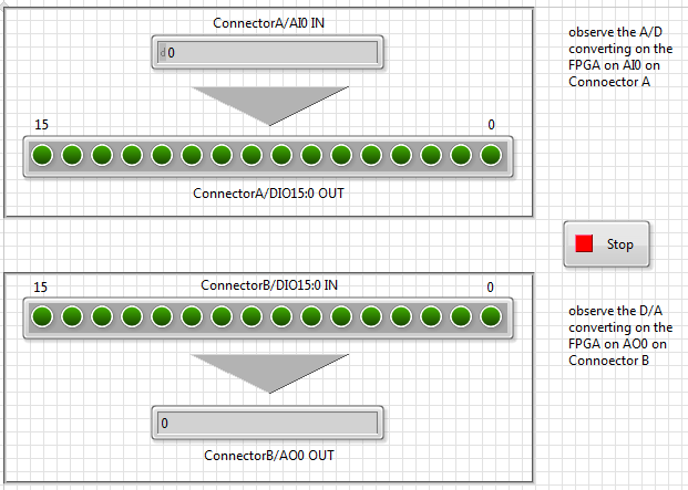
The RT VI DACandADC-Observer.vi is just using Read-Write-controls towards the FPGA VI to display the DAC and ADC operation on the front panel.
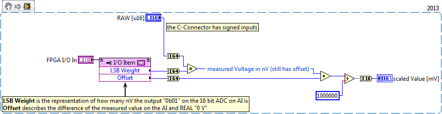
Please note, that the analog values on the front panel are unscaled RAW input values of the myRIO. Have a look at this snippet on how to perform the scaling (it is taken from the myPID example, where I pointed out, that this VI should probably used on the RT, rather then on the FPGA since it is ressource-eating and it's only purpose is to scale the values for the user to readable values):
The following snippet shows the FPGA code, where the ADC and DAC operations take place. Note, that one can read and write to a bank of 8 DIOs at once by using a U8-number for the whole port! This makes the FPGA code very easy and small:
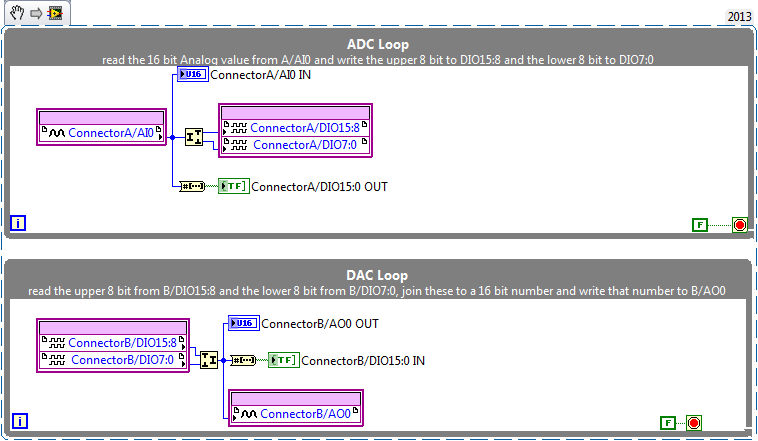
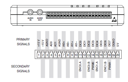
ADC on Connector A
As you can see, the DIOs 15:0 on Connector A are used as digital outputs of the analog-digital-converted value of AI0 on Connector A
DAC on Connector B
The DIOs 15:0 on Connector B are used as digital inputs to be converted into an analog value, outputted on AO0 on Connector B
Product Marketing Manager for CompactRIO & TSN
Making the intangible, tangible
- Mark as Read
- Mark as New
- Bookmark
- Permalink
- Report to a Moderator
Could you measure ADC-DAC responce time with external oscilloscope ?
ext signal (meander) -> (ADC-myRIO-DAC) -> ext scope chan1
ext signal (meander) -> ext scope chan2
What's the difference (ms/us)?
Is it a constant value?
p.s. maybe you know:
Is ADC/DAC connected to PS or PL part of Zynq IC in myRIO ?
thanks a lot!
