- Subscribe to RSS Feed
- Mark Topic as New
- Mark Topic as Read
- Float this Topic for Current User
- Bookmark
- Subscribe
- Mute
- Printer Friendly Page
FPGA code to sample an NI-9205
Solved!01-23-2018 10:11 AM
- Mark as New
- Bookmark
- Subscribe
- Mute
- Subscribe to RSS Feed
- Permalink
- Report to a Moderator
Hi All,
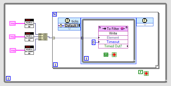
I've inherited some FPGA code that samples 16 voltages from a NI-9205 with an FPGA I/O node and feeds them into a FIFO. The FPGA I/O node is called in a standard infinite while-loop and passed through a unit delay node, see below. What is the purpose of the unit delay? The FIFO gets called in the same loop, but is buried inside of a single-shot single-cycle-timed-loop (SCTL) inside of a for-loop. How is the SCTL behaving? I believe the SCTL is using the 40MHz system clock. Since while loops are pretest loops, my guess is that the outer loops are much faster, and it effectively behaves like an infinite SCTL sampling from each channel at 40/16=2.5MHz. The NI-9205 doesn't sample nearly that fast, so I'm getting sample-and-hold data (with a lot of hold). Thoughts? Thank you!
Solved! Go to Solution.
01-23-2018 12:49 PM - edited 01-23-2018 12:50 PM
- Mark as New
- Bookmark
- Subscribe
- Mute
- Subscribe to RSS Feed
- Permalink
- Report to a Moderator
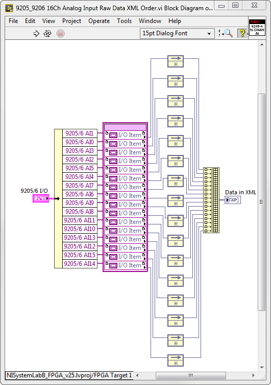
The feedback node is to pipeline the ADC management from the upstream for loop. You'd have near identical code if you moved it outside the build array or outside the subVI.
The SCTL is almost useless. It will contrain whatever is inside to only use one cycle but it's not going to magically break dataflow and ignore the outer for loop. There's an equal chance it improves, worsens, or does nothing to the amount of resources the bitfile is using.
01-24-2018 08:52 AM
- Mark as New
- Bookmark
- Subscribe
- Mute
- Subscribe to RSS Feed
- Permalink
- Report to a Moderator
Nanocyte - Thank you! Couple of followup questions:
1. Can you elaborate on "pipeline the ADC management". I saw a note about this here but didn't understand at that time either.
2. I discussed with a coworker, and a missing piece in my understanding is that FPGA I/O node actually waits (possibly yielding execution) until a complete set of new samples from all of the 9205 channels is available. Can you confirm this and maybe point me to some documentation with more details?
Thanks again!
01-24-2018 10:38 AM
- Mark as New
- Bookmark
- Subscribe
- Mute
- Subscribe to RSS Feed
- Permalink
- Report to a Moderator
Yes, that is a critical piece of information. That IO node is not a single cycle operation. Check out the context help which will usually mention that. The IO node takes many cycles to operate. The best way to figure out how many is to benchmark it using the tick count. Following LabVIEW's dataflow law, nothing upstream can run until it finishes executing. The work around for that is to put the dataflow through the feedback node. Since everything prior to the node happened in the previous loop iteration, the execution of the items upstream happens in parallel although using information that's one iteration old.
01-24-2018 11:30 AM
- Mark as New
- Bookmark
- Subscribe
- Mute
- Subscribe to RSS Feed
- Permalink
- Report to a Moderator
When you say "until it finishes executing", does "it" refer to the "FPGA IO Node"?
Ah (light bulb going off), okay, if that is the case, that makes sense then.
I googled around for "LabVIEW's dataflow law" and saw some good articles about data flow in graphical programming (interesting to me b/c I'm just a year into LabVIEW and I come from a background of lower level embedded realtime C), but nothing specifically on FPGA IO node data flow. I also checked out LabVIEW context help on FPGA IO Node, but nothing there either. Can you point me to an article?
01-24-2018 12:11 PM - edited 01-24-2018 12:31 PM
- Mark as New
- Bookmark
- Subscribe
- Mute
- Subscribe to RSS Feed
- Permalink
- Report to a Moderator
Yes, I was referring to the IO node but dataflow as a concept is applicable to nearly every node. The article you linked to is a good introduction.
This is the relevant help doc for your particular IO node. The behavior is hardware specific:
http://zone.ni.com/reference/en-XX/help/370984R-01/criodevicehelp/crio-9205/
Note where it says: This device does not support the single-cycle Timed Loop.
That's telling you it takes multiple cycles to complete. The LabVIEW compiler takes care of the enable circuitry to disable the upstream elements while the downstream nodes are enabled. When you put the feedback node down, you're telling LabVIEW to create a set of registers to hold the data so that the upstream stuff has its own copy so that both can be enabled at the same time.
01-24-2018 01:04 PM
- Mark as New
- Bookmark
- Subscribe
- Mute
- Subscribe to RSS Feed
- Permalink
- Report to a Moderator
I did see that article and did wonder about the incompatibility with single cycle timed loops. Its all coming together for me now.
I do remember reading about timed loop constraining to a single cycle in FPGA context. So you are thinking that somebody (I'm told this is actually legacy code originating from NI many years past) put it there possibly thinking it would reduce the amount of resources. I was focused on the potential affect on timing and hadn't thought about the ancillary benefit of single cycle constraint.
Its clear to me that the SCTL doesn't affect the timing of the actual hardware samples, but it seemed to me that perhaps it may have some (pointless) impact on the timing of the queuing. By single-cycle, I'm guessing there is clock signal that perhaps drives something like a high priority task executing at a single tick rate. Could this SCTL have the affect of limiting the queuing to one sample per cycle? I see your point, though, why wait?
01-24-2018 02:23 PM - edited 01-24-2018 02:26 PM
- Mark as New
- Bookmark
- Subscribe
- Mute
- Subscribe to RSS Feed
- Permalink
- Report to a Moderator
I may have started leading you astray. At no point was I talking about the single cycle loop in your code. I thought you might be confused about which nodes take multiple cycles to calculate and which don't and I was showing you what to look for.
Regarding your actual single cycle loop—it does one thing for sure: it specifies that the code inside has to meet the base clock timing constraint. That constraint likely amounts to nothing as it already would have executed in one cycle. Furthermore, you don't need it to complete in one cycle, the loop rate limiting step is the ADC so who cares. The other thing it might do is provide resource optimization. My guess is that it doesn't and you should get rid of it. If you wanted to verify that you'd compile it both ways and check your resource usage.
01-24-2018 02:29 PM
- Mark as New
- Bookmark
- Subscribe
- Mute
- Subscribe to RSS Feed
- Permalink
- Report to a Moderator
Thanks Nanocyte! You communicated very clearly an otherwise complicated subject and really helped me to get a grasp about what is going on. Thank you. I marked your last reply as solution and Kudo'd all the way through. Thanks again!
01-25-2018 04:22 PM
- Mark as New
- Bookmark
- Subscribe
- Mute
- Subscribe to RSS Feed
- Permalink
- Report to a Moderator
Sorry, one more "teeny" question... you mentioned "ADC". Does ADC mean analog-to-digital converter? -- Thanks 🙂


