- Subscribe to RSS Feed
- Mark Topic as New
- Mark Topic as Read
- Float this Topic for Current User
- Bookmark
- Subscribe
- Mute
- Printer Friendly Page
Phase Shifted Carrier Signals For FCM applications
01-30-2016 04:05 PM
- Mark as New
- Bookmark
- Subscribe
- Mute
- Subscribe to RSS Feed
- Permalink
- Report to a Moderator
I need to build phase shifted carrier signals for application to a five-level flying capacitor multilevel inverter on the 9606-GPIC. I think fixed point might suffice, but I'd still prefer to use floating point for the controls.
In order to build the 4 carrier signals, I can think of the following two ways.
1) create 5 copies of the triangle generators within a SCTL and hardcode phase shifts of 2*pi/n between two carriers. Also create a slower derived clock (say ~5Mhz) and run the SCTL at this rate so that there's enough time for the code with it to run at this speed (with determinism)
2) Use one triangle generator (or maybe even two if the FPGA can handle it) and use discrete delay blocks for phase shifts to create 4 of the other carriers.
I can think of a few problems that I might run into with each of these methods,
1) I will use a lot of FPGA resources to create 5 seperate triangle generators within one SCTL, and also I probably can't use the reentrant subVIs for the floating math
2) I will use too much memory space with the delay block method because I will basically be storing the entire values of the carrier waves.
Does anyone have some experiences that they could share with me regarding implementing 4 phase shifted carriers? I would appreciate any suggestions or design examples on this topic.
02-01-2016 02:28 AM
- Mark as New
- Bookmark
- Subscribe
- Mute
- Subscribe to RSS Feed
- Permalink
- Report to a Moderator
Hi Athapa,
I come from DSP experience and in that case the PWM unit has only a single carrier. So, the modulating signal must be split when a modulator for multilevel converter is needed.
Hence, instead of using different carriers you could try to split the modulating signals according to the threshold which are mainly based on the carriers edges.
Please have a look to the attached PDF.
I do not know if it will save FPGA space, but you could try.
However, to generate the carrier signals use the minimum data-width, for instance FXP with integer value only, instead of Uin16 etc...
Cheers,
AL
02-01-2016 09:56 AM
- Mark as New
- Bookmark
- Subscribe
- Mute
- Subscribe to RSS Feed
- Permalink
- Report to a Moderator
hello AL3,
Thanks for your response.
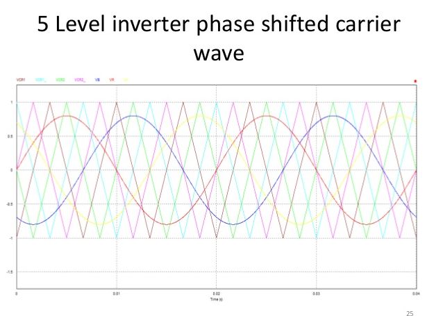
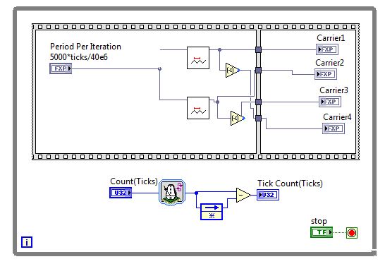
What's shown in the pdf you attached is "level-shifted carriers." It's the most popular modulation technique in multilevel converters. However, one of its drawbacks is unbalanced capacitor voltages. The technique I want to implement is a "phase-shifted carriers" which has the property of automatically balancing the capacitor voltages. So I would need seperate carrier signals. For a five level converter I require 4 carrier signals phase shifted by 90 degrees. I was able to attain this by the code shown below.
Since this strategy would require active capacitor voltage balancing, I also will require enough resources to implement this on the FPGA. I haven't done it yet but I am already worried that I might not be able to fit all of it.
02-01-2016 11:01 AM
- Mark as New
- Bookmark
- Subscribe
- Mute
- Subscribe to RSS Feed
- Permalink
- Report to a Moderator
I recently created a 3ph Interleaved DC/DC PWM signal generator for some internal testing that used three triangle generators with inputs for setting initial conditions to create the necessary phase shift.
I used the “3-Phase DC-to-DC Converter” example within the GPIC Reference Design (LabVIEW 2014) as a starting point. The triangle generator was based on the existing “[FPGA] FXPT TriangleGen with Mod Index (use inside SCTL)” vi, but modified to accept an “Initial Count Value” and an “Initial Count Direction” parameter. Three copies of this vi are placed in the top-level FPGA vi and each wired with appropriate initial conditions to generate the three phase-shifted triangle waves.
This is the triangle generator vi (attached). I also modified it to count between 0 and 1 and deleted some unneeded code from the original version.
![[FPGA] FXPT TriangleGen (use inside SCTL).png](http://forums.ni.com/legacyfs/online/196197_[FPGA] FXPT TriangleGen (use inside SCTL).png)
This is how the three triangle generators are wired in the top-level FPGA vi:
![[FPGA] GPIC 3-Phase Interleaved DC-to-DC Converter Control.png](http://forums.ni.com/legacyfs/online/196198_[FPGA] GPIC 3-Phase Interleaved DC-to-DC Converter Control.png)
This code (along with the rest of the code that is part of the FPGA reference design) fit onto an sbRIO-9606 with room to spare.
You could check to see if your code will fit on the FPGA without having to compile it using the "Estimate Resource Usage" function.
02-01-2016 11:47 AM
- Mark as New
- Bookmark
- Subscribe
- Mute
- Subscribe to RSS Feed
- Permalink
- Report to a Moderator
Hi Athapa,
the attached image is the main scheduler I use on the FPGA. Simmetrical carrier generation, resouce usage negligible.
For instance, a full PM-machine vector control on a 3-phase IGBT inverter with current loops, speed loop, desaturation, voltage vector saturation, measure acquisition and scaling, generating proper modulating signals, CAN-bus and RS-485, resolver management etc... takes around:
Slice LUTs 23%
Block RAMs 5 %
DSP48s 16%
on a ZYNQ-7020 (sbRIO9651)
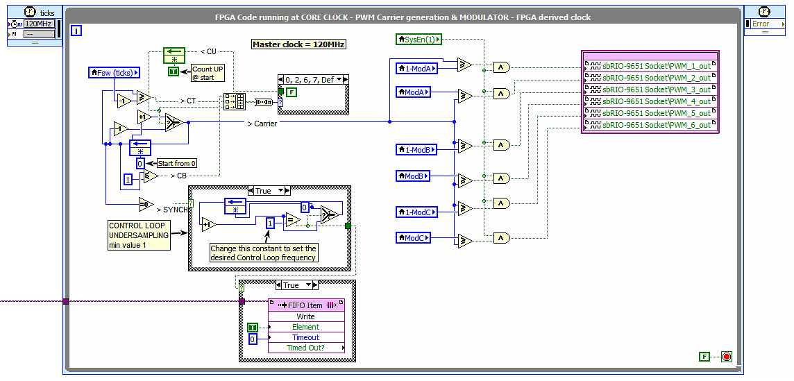
Hence, you can generate the carriers you need...unless your FPGA is very very small.
BTW, in a NPC multilevel inverter, good capacitor balancing can be obtained injecting a homopolar component in the modulating signals (i.e. 3rd harmonic).
02-01-2016 11:56 AM
- Mark as New
- Bookmark
- Subscribe
- Mute
- Subscribe to RSS Feed
- Permalink
- Report to a Moderator
That's awesome!
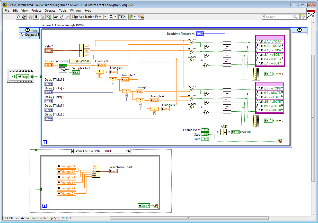
Here is one more option- to use FPGA RAM FIFOs to phase shift the carriers. It is a pretty light option in terms of FPGA resource consumption. In this case, the sine-triangle PWM loop is floating point and running at 40 MHz, so I'm using the floating point Variable Depth FIFO.vi. You can find this IP core in the master IP and examples library here:
C:\LabVIEW 2015\IP Cores\IP Cores - LabVIEW FPGA\Floating Point\Variable Depth FIFO.vi
Below is a screenshot of the FPGA simulation testbench running (the chart indicator is only enabled in simulation mode.) In this case the carrier frequency is 11.1 kHz (3600 ticks at 40 MHz) and there are 6 interleaved carrier waveforms, so the phase shift for each is 3600/6 = 600 Ticks. The Carrier Frequency register value is calculated as fc(Hz)*8*dT = 11.1e3*8/40e6 = 0.00222222.
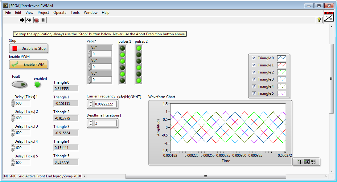
FPGA control application in simulation mode (FPGA_EMULATION=TRUE):
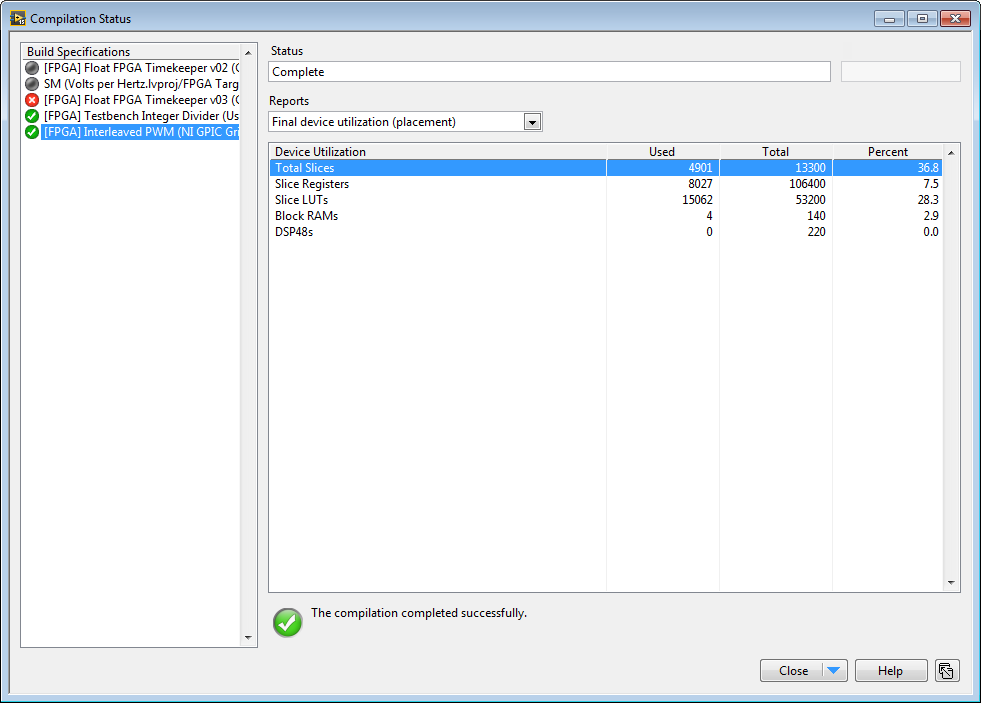
Compile report. Note the FPGA RAM usage (4 out of 140 Block RAMs). The other Slice resource usage values are not very reliable since the FPGA is not close to full- therefore the compiler will not "try hard" to make it fit.
Notes:
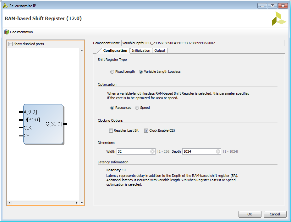
- The floating point Variable Depth FIFO IP core is based on the Xilinx Coregen RAM-based Shift Register.
- For information on the FPGA resources consumed, see here.
- This IP core is limited to a depth of 1024 samples. If deeper FIFOs are needed, you can run your PWM single cycle timed loop at a lower clock rate or create your own FIFO using LabVIEW FPGA RAM functions. When using LabVIEW FPGA RAM Read/Write functions, you can read or write multiple channels of data in a single clock cycle if you use a cluster with a custom data type control.
- When using the Xilinx Coregen core, you can configure it for other data types as needed if desired.
- One nice benefit is that there is zero latency, which makes programming as shown above very easy.
- Here is a screenshot of the coregen configuration (to get here, open the Variable Depth FIFO.vi, right-click the Coregen block and go to Properties, then click Configure Xilinx IP).
The code above is uploaded here:
ftp://ftp.ni.com/evaluation/powerdev/training/InterleavedPWM.zip
After downloading, you can find the FPGA VI above here:
C:\LabVIEW 2015\GPIC\GPIC Grid Active Front End\[FPGA] Interleaved PWM.vi
02-22-2016 02:19 PM
- Mark as New
- Bookmark
- Subscribe
- Mute
- Subscribe to RSS Feed
- Permalink
- Report to a Moderator
I'm putting together a Grid-tied bidirectional inverter and I'm writing the codes in labVIEW. I have come to realise that using arrays in labview makes programming easier. Does using Arrays take up more FPGA resources as opposed to handing the individual variables?
02-22-2016 09:35 PM
- Mark as New
- Bookmark
- Subscribe
- Mute
- Subscribe to RSS Feed
- Permalink
- Report to a Moderator
Hi Athapa
That's a good question. Let's focus on FPGA, each control or indicator has its own overhead. Probably using an array would be better.however the address of the array element seems to be i32, which is not efficient: I do not know how Labview manages it.
We should understand deeply how the array in placed n the FPGA because in a microprocessor is just a starting memory address, which make the usage very effective.
Cheers,
AL3
BTW, with reference to the starting td, the control board I am using is this one www.ped-board.com
02-24-2016 11:17 AM
- Mark as New
- Bookmark
- Subscribe
- Mute
- Subscribe to RSS Feed
- Permalink
- Report to a Moderator
Short answer: Small arrays (< 20 elements) in LabVIEW FPGA are okay but take a lot of resources. Large arrays (> 20 elements) will take too many resources. Arrays used on the block diagram take much fewer resources than arrays with front panel controls or indicators. (I explain why below.)
A better, more efficient and more powerful way is to use an FPGA RAM register using the VI Defined Memory functions. This enables you to efficiently create large "arrays" (> 1000 elements), and also provides an easy to use addressing scheme (like a pointer) that is very powerful. Also, there are powerful tools to initialize the FPGA RAM items if a single data type is used (i.e. floating point) to implement custom math functions, etc. (I'll show how below.) Furthermore, in the case of an FPGA RAM Memory that uses a custom control typedef cluster, all memory elements can be read in a single clock tick rather than taking one clock cycle per memory item. That is a big speed advantage. However, if you use a cluster, you must initialize the memory values in run time if you need initial values that are not the default (i.e. 0 for floating point, false for Boolean, etc.). Thus, when speed is really important such as in my high speed multichannel floating point transfer function (which executes at around 6 MHz for a first order system), I use a custom data type cluster to provide a high bandwidth interface to multiple memory items. It takes just one clock tick to read all of the items.
Why do front panel controls/indicators for arrays take a lot of FPGA resources? Creating a front panel control or indicator in LabVIEW FPGA for an array or cluster does three things. First, it creates an internal FPGA register for holding and sharing data within the FPGA application through local variables. Second, it creates a communication register than can be used for passing data back and forth with the Real-Time operating system. Third, it ensures that read/write access to the array or cluster items is synchronous. In other words, any accessor that's writing the array or cluster must update all elements simultaneously. Any accessor that's reading the array or cluster will be ensured that the values were updated simultaneously, and won't get a partially updated result in the case that values are being changed by a writer. This can be a powerful and useful feature, but it also means that there is a significant amount of FPGA resources utilized to handle the arbitration. That's why arrays and clusters take a lot of resources when they become large.
On the other hand, with FPGA RAM "arrays" the individual items can be written and read on any clock tick so there is no synchronous updating of the elements in every memory address. This can enable powerful capabilities too. In the case of FPGA RAM clusters, all of the cluster items at a single address are updated synchronously (on the same clock tick), but the cluster data values located at different memory addresses are not updated synchronously.
Also, FPGA RAM offers dual port access capability for very high speed applications but I won't go into that here because it's not commonly used in embedded control applications.
Let me show an example of how powerful using FPGA RAM can be rather than front panel array controls/indicators.
I am working on a Proportional Resonant Controller with Harmonic Compensation, and I wanted to try using an inverse notch filter rather than the traditional resonant transfer functions you find in papers on PR control. I will calculate the filter coefficients for each harmonic frequency and initialize the FPGA RAM with the correct values. In that way, my calculations for the filter coefficients can be very complex, but only the calculated value is stored so the FPGA implementation is extremely efficient.
The inverse notch filter discrete time equations are the following:
Inverse Notch Filter:
u
y
where
BW = (1-r)/2
alpha = -(1+r)*cos(2*pi*Fo/Fs)
r = (1+cos(2*pi*K/Fs)-sin(2*pi*K/Fs))/
(1+cos(2*pi*K/Fs)+sin(2*pi*K/Fs))
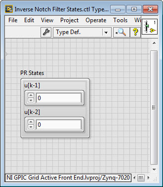
Fo [Hz] represents the frequency at which the inverse notch filter allows the energy to pass, Fs [Hz] represents the sampling frequency at which the IP core executes, and K [Hz] represents the width of the notch filter passband. There are two state values, u[k-1] and u[k-2], that must also be held in memory for each harmonic frequency.
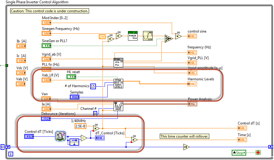
Here is my FPGA IP core that implements the filter.

To create the FPGA RAM register for the single precision floating point state values, u[k-1] and u[k-2], I first create a cluster and right-click on it to make it a custom data type. Then I save it as a .ctl file.
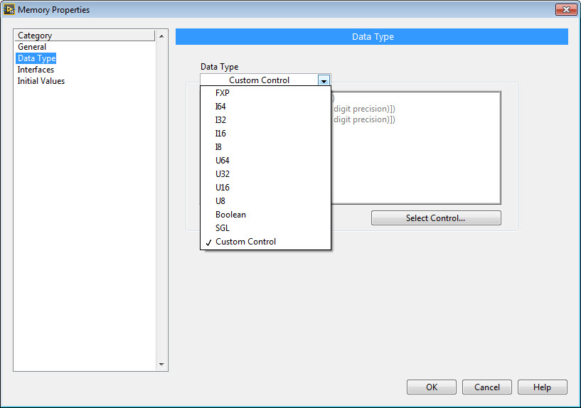
Next I drop down the VI-Defined Memory Configuration item from the LabVIEW FPGA Data Storage & Transfer palette, and double click to configure it. On the Data Type tab I select Custom Control and navigate to the custom control .CTL file that I just created.
For these states, the default values for the data type (value = 0) are what I want, so it is not a problem that I cannot initialize the RAM values to something else when using a cluster. I'm using a cluster for the speed of accessing the memory. Note that it doesn't pack as efficiently into FPGA RAM as values of a single data type, so if I'm really concerned about running out of RAM I might not use a cluster.
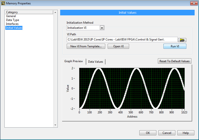
Next I drop down VI-Defined Memory Configuration registers for the alpha, r and BW filter coefficients. I set the data type to SGL (single precision floating point) and go to the Initial Values tab. Then I click New VI from Template... to generate a template for me to use to initialize the RAM memory values. Or if, you've already defined the initialization VI, you can click Open VI.
Here is the initialization VI for the inverse notch filter alpha coefficients. It stores 1024 values, beginning with an Fo value of 0 Hz, then 60 Hz, 120 Hz, 180 Hz, etc. So it starts at DC and goes all the way to the 1023 harmonic of the grid frequency. (In practice, going to the 100th harmonic or so would be sufficient.) Inside the For Loop I have a Formula Node, which allows me to enter the equations for the filter coefficients in the C language syntax. The array that initializes the FPGA RAM must have the caption "Init Data Out", so don't change that caption. In the screenshot below it's the array indicator that is not labelled.

Once your initialization VI is ready, you point to it in the RAM initialization page and click Run VI. Now, when the FPGA is compiled, these values will be loaded as a the default values for the RAM.
Note that because these RAM initialization filter coefficient values include the sampling rate at which the filter executes, in this case 45 microseconds or 1800 clock ticks, it is very important to ensure that it does execute at the intended rate when the FPGA is compiled and running. Therefore, I measure the loop rate in the FPGA application in which it is used, and also make a note of the design loop rate in the VI icon as shown below. Alternately, I could pass the FPGA RAM memory reference to the top level FPGA application, and add a loop that let's the values be written to in run time by the RT application.
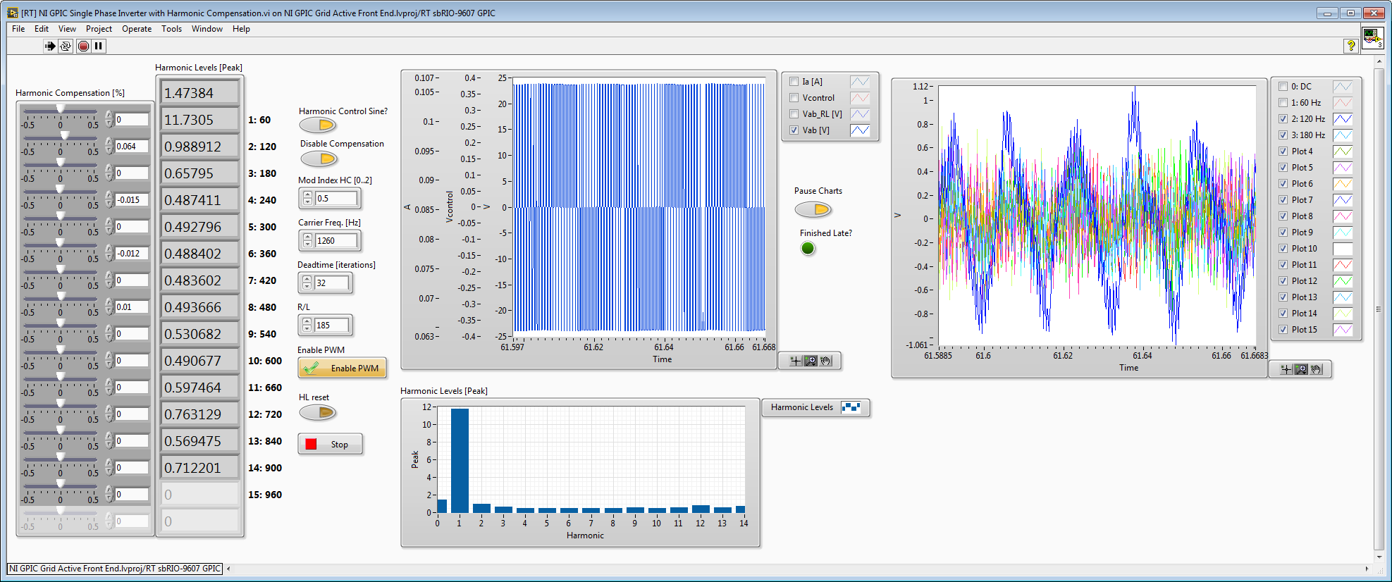
What's really important for development productivity is to always create a simulation testbench application to test your code before you compile. Here is the testbench application. It shows that the inverse notch filter is able to recover the original harmonic voltage waveforms without changing the amplitude or phase shift.

I recorded a video of testing the inverse notch filter for harmonic level detection using a digital twin observer for the inverter line reactor filter and load, which you can see here if you are interested. Based on these initial tests, the inverse notch filter seems to be working extremely well. You can download the code shown above from here, which includes the fix to the bug in my multichannel peak level detector IP core found in the testing video.
The screenshot below shows the actual recovered harmonic waveforms for an actual inverter running with sine-triangle PWM. This too cool. This is using the output of the digital twin RL line reactor filter model—the input to the inverse notch filter is the actual measured IGBT half-bridge voltage (line-to-line). The recovered harmonic voltage waveforms are even in phase with the original Vab_RL

Here it is fed with the measured IGBT half-bridge voltage (line-to-line) without the LR transfer function observer. As you can see, the higher order harmonics are not attenuated.
03-10-2018 01:47 AM
- Mark as New
- Bookmark
- Subscribe
- Mute
- Subscribe to RSS Feed
- Permalink
- Report to a Moderator
There is an error when trying to use the FPGA RAM FIFO's with LabView 2016. I was getting the error below.


The graphic above illustrates Ram Based Shift register on the block diagram of the Variable Depth FIFO. In order to get this to work as a sub VI in a SCTL, the SCTL Timed Loop Frame has to be removed from the frame. Once this was done the error went away.
