- Subscribe to RSS Feed
- Mark Topic as New
- Mark Topic as Read
- Float this Topic for Current User
- Bookmark
- Subscribe
- Mute
- Printer Friendly Page
GPIC Interface Board PCB with Dual SEMIKRON SKiiP3 26-Pin Ribbon Connectors (open source design files attached)
08-10-2012 07:03 PM
- Mark as New
- Bookmark
- Subscribe
- Mute
- Subscribe to RSS Feed
- Permalink
- Report to a Moderator
SVTRONICS has the latest revision of these open source interface PCBs in stock and available for ordering worldwide. Please contact Chris Dickey at SVTRONICS (chris@svtronics.com, Tel: 214.440.1234 x102) and reference the "SEMIKRON SKiiP3 Dual 26-Pin Interface PCB for NI GPIC."
Note that the interface design is open source and is intended to be a starting point for full scale power converter interface board designs. For example, if your application utilizes SEMIKRON SEMIKUBE power converters, you would modify the 26-pin SKiiP3 ribbon cable connectors to match the 34-pin SEMIKUBE pinout. The board also includes screw terminal connectivity for the GPIC I/O, which is ideal for rapid prototyping. For production, the screw terminal connectors are typically replaced with mass termination connectors (i.e. ribbon cable or DSUB connectors) and the mechanical design of the board is adjusted to meet the exact application specific requirements for the converter cabinet.
Below are details on the latest revision of the open source template design.
Update September 4, 2014:
- Updated schematic, layout and bill of materials (BOM) is attached. Added jumpers to enable certain analog inputs to be disconnected from ground when not using SKiiP3 connectors, to allow connection of external differential analog input sensors. Increased package size of surface mount resistors for easier hand soldering. Miscellaneous silkscreen updates. Updated BOM with recommended SKiiP3 connectors (3M 3429-6002).
- We are pleased to announce that SVTRONICs will begin building in quantity and holding stock to facilitate small orders with short lead time.
- Note: Be sure to request >= 93 mil PCB thickness when ordering from your PCB house.
NI GPIC INTERFACE PCB FOR DUAL SEMIKRON SKiiP3 26-PIN RIBBON CABLE CONNECTORS
Read a whitepaper about this design:
NI Ultiboard Design of a GPIC Mating Board
Latest Version: Revision 2, Version v03
Revision 2, Version v03 Notes:
- Two 26-pin interface connectors located on the bottom side for direct ribbon cable connection to Semikron SKiiP 3 or Methode SmartPower Stack™
- Channel assignments identical to the GPIC Inverter Research Board- move from small scale prototyping to full scale inverter control with only minor changes to gains, offsets and limits
- For example code based on this interface board and a Semikron SKiiP 3 six pack (3-phase DC to AC) inverter, see the following post:
Example Code: Getting Started with the NI Single-Board RIO General Purpose Inverter Controller (GPIC...
Description
- Caution: Template design not verified for production. No gaurantees of performance are provided.
- Caution: The NI 9683 is designed for low voltage signals. You must ensure that your mating board circuitry and sensors provide sufficient safety isolation to ensure no unsafe voltages are present at the inputs to the NI 9683. Voltages that exceed the specifications could result in damage to the NI 9683.
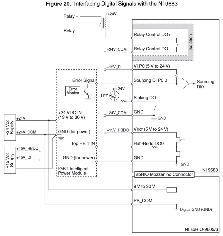
SYSTEM GROUNDING RECOMMENDATIONS
System Grounding Recommendations:
- +24 VDC Power Supply Connections (Main Controller Power)
- Connect +24V power to +24Vdc IN on the Semikron IGBT 26-pin connector
- Connect +24V power to input power supply of the sbRIO
- Connect +24V GND/COM to GND input on the Semikron IGBT 26-pin connector
- Connect +24V GND/COM to GND (Digital GND) input power supply of the sbRIO
- Connect +24V Earth (chassis) ground to system Earth (chassis) ground
- +15 VDC Power Supply Connections (Gate Driver Control Signal Power)
- Connect +15V power to Vext input on the NI 9683
- Connect +15V GND/COM to GND input on the Semikron IGBT 26-pin connector
- Connect +24V Earth (chassis) ground to system Earth (chassis) ground
- ±15 VDC Sensor Power Supply Connections (Sensor / Transducer Power)
- Connect ±15 power to system sensors/transducers
- Connect ±15 GND/COM to CS_COM input on the NI 9683
NOTE 1: Do not connect ±15 sensor GND/COM to any other system ground other than CS_COM.
NOTE 2: Do not use the 15V sensor power supply as the gate driver control signal power supply.
- Other Grounding Connectivity:
- Connect Semikron IGBT power stack heat sink to Earth (chassis) ground
- Connect sbRIO chassis ground metal terminal to Earth (chassis) ground
- Connect the shield of the cable interfacing the Semikron power stack to your custom interface board to Earth (chassis) ground
FEATURES OF THE EXAMPLE BOARD
- Open source design for use as an evaluation, testing & signal breakout board
- Can be modified to create your custom user defined GPIC interface board. See section below titled "TYPICAL USER DEFINED MATING BOARD FUNCTIONALITY".
- Export the Gerber files from Ultiboard (File>Export) and send to the PCB fabrication/assembly house of your choice
- Female IDC headers for mating to the NI 9683 GPIC located in proper mechanical position with signal names labelled on silkscreen
- Screw terminal breakout connectors for each GPIC I/O connector
- Dual 26-pin IDC connectors compatible with Semikron SKiiP 3 and Methode Smart PowerStack
- Powered by external 15 VDC regulated supply with extra terminals for jumpering power to the sbRIO-9606 using the 2-position mini-fit power plug pigtail wire assembly (NI Part #: 152834A-01)
- Shunt resistor pads for all analog inputs (surface mount size 2512) enable conversion from voltage to current sensing analog inputs
- Preservation of ground plain and trace keepout spacing distances for functionally (not safety) isolated simultaneous AI and relay control DO signals
- LVTTL connector trace widths and PCB material intended for 55 Ohm signal impedance
- Follows Simultaneous Analog Input psuedo-differential grounding scheme recommendations (see OEM design file "Readme - NI GPIC Mechanical and Mating PCB Info v0_.docx")
- Thick 0.093" PCB for mechanical strength
- 0.040” plated holes for the SH2 mating connectors for proper IDC connector mechanical alignment
- Keepout spacing on all sides suitable for extraction crowbar tool
- Keepout area for HALO transformer (no components should be placed underneath)
TYPICAL USER DEFINED MATING BOARD FUNCTIONALITY
Your custom mating board maps the GPIC I/O to your connectors of choice and typically includes things like the following:
- Cable interface connectors. Shielded twisted pair cabling with proper cable and termination impedance is recommended.
- Signal conditioning. This often includes shunt resistors for sensors with a current output signals, like LEM current sensors, which should be placed as close as possible to the GPIC analog inputs.
- Watchdog timer circuitry. If the NI GPIC FPGA does not toggle the watchdog timer signal for, say 10 microseconds, then set your gate drivers to open all power transistors. Designing your inverter control system for fail safe operation is critical. We also recommend programming the LabVIEW FPGA and LabVIEW Real-Time processors to include watchdog timers in both directions.
- Gate signal feedback circuitry. This enables you to monitor the status of the gate command signals coming from the NI GPIC RMC. Alternately, some customers choose to use special isolation circuitry to monitor the actual gate drive signals which enables you to detect any failure in the path.
- Gate drive circuitry. It's more common now to use gate driver boards that mate on top of the IGBT module, so in that case you would cable the High Speed DO outputs from the GPIC mating board to the gate driver board or Intelligent Power Module.
- Power supply DC/DC converters, if needed to step down a voltage to 24 VDC to power the GPIC and/or other circuitry at different DC voltage levels- for example, stepping down the battery voltage on an electric vehicle, or stepping down grid voltage after rectification.
MECHANICAL CONSIDERATIONS
- The trace width on the relay control digital output traces should be designed to handle the 8 Amp inrush capability of the GPIC relay control digital outputs. You must also use external flyback diodes to protect the relay control outputs and ensure your cabling to the contactor relays has sufficient current handling ampacity. For more information, see the topic "Protecting the Relay Control Digital Outputs from Flyback Voltages" in the NI 9683 user manual.
- There are some special considerations for the stand-offs, which are not standard dimension. The drawing includes the correct stand-offs. Here are the details:
- 4 standoffs used to mount sbRIO to GPIC require a custom standoff length of 0.380 inches (9.65 mm).
- It is recommended to use an M3x9.65 mm length, M4.5 HEX or a 4-40x0.380 inch length, 3/16 HEX standoff, with a precison tolerance of +/-0.002 inches
- This is required per the high density RMC connector manufacturer (Samtec), to prevent damaging the connector from overmating.
When using a user defined mating board to connect to the GPIC board:
- It is recommended to use a 4-40x0.437 inch length, 3/16 HEX standoff to mount GPIC to the 3rd board.
- Use caution when un-mating the 3rd board from GPIC, and be sure not to un-mate at an angle. This could cause damage to the pins or connector shrouds.
- An ejector tool for separating the sbRIO-9606 and 9683 GPIC mezzanine card is available. Once mated, the retention force of the 5 0.1" pitch ribbon connectors is high. We recommend one time connection only, however, we do have a special crowbar tool from our 3D printer that we can provide which will enable you to separate from the GPIC RMC without damage if required.
USER DEFINED MATING BOARD PCB DESIGN MECHANICALS
- Refer to the NI 9683 operating instructions and user manual for dimensional drawings. The manual also contains recommended mating connectors.
- Extra thick board thickness PCB is recommended for mechanical strength: 0.093 inch thickness is recommended.
- It is recommended to use 0.040” plated holes for the SH2 mating connectors. This is to prevent the connectors from being placed at an angle, and to ensure proper mating to GPIC.
PSUEDO-DIFFERENTIAL SIMULTANEOUS ANALOG INPUT GROUNDING SCHEME
The Simultaneous Analog Input section of the NI sbRIO GPIC is functionally (not safety) isolated from the other sections of the board, and the differential channels are pseudo-differential. The design was done this way to match the pseudo-differential outputs of the Semikron module, and is generally the lower cost approach to such a circuit. However, because the channels are pseudo-differential, maintaining good common mode rejection requires careful attention to grounding. The Semikron module has a chassis terminal that is shown connected to their board's ground in the SKiiP 4 application note; however, this will defeat the common mode rejection. See the grounding scheme diagram below for more details.
Notes:
- The + 15 VDC OUT auxiliary power supply on the SKiiP 3 is limited to 50 mA max, and therefore is not suitable for powering the NI sbRIO GPIC Half-Bridge Digital Outputs (J3).
System Diagram (Semikron SKiiP and LEM Sensor Example):
Notes: Updated versions of the diagrams below are now included in the NI 9683 GPIC user manual. Please refer to the NI 9683 user manual for information on this topic.
IMAGES
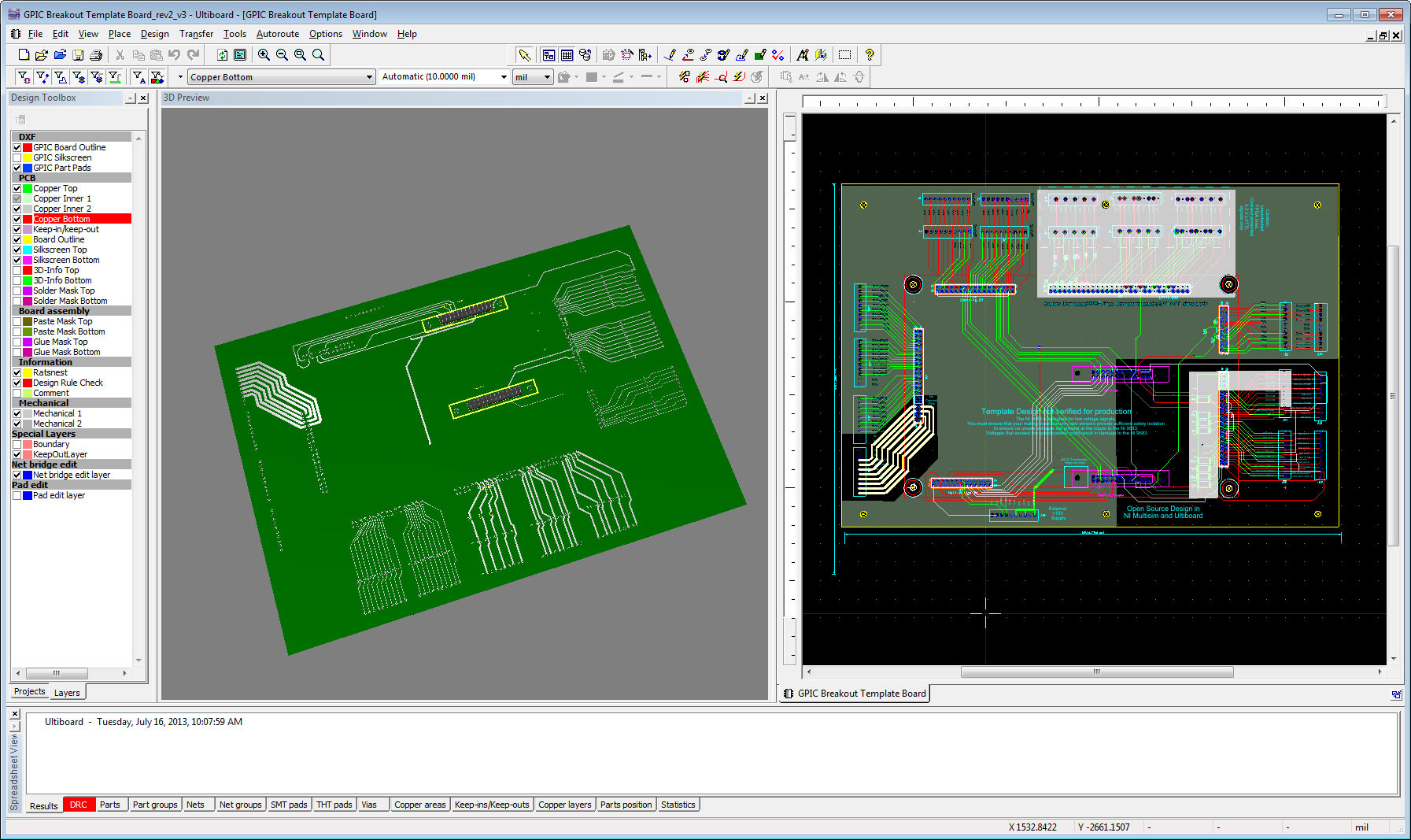
Ultiboard PCB layout:
TOP (IDC headers for NI sbRIO GPIC, screw terminals for I/O signals and power, shunt resistor pads):
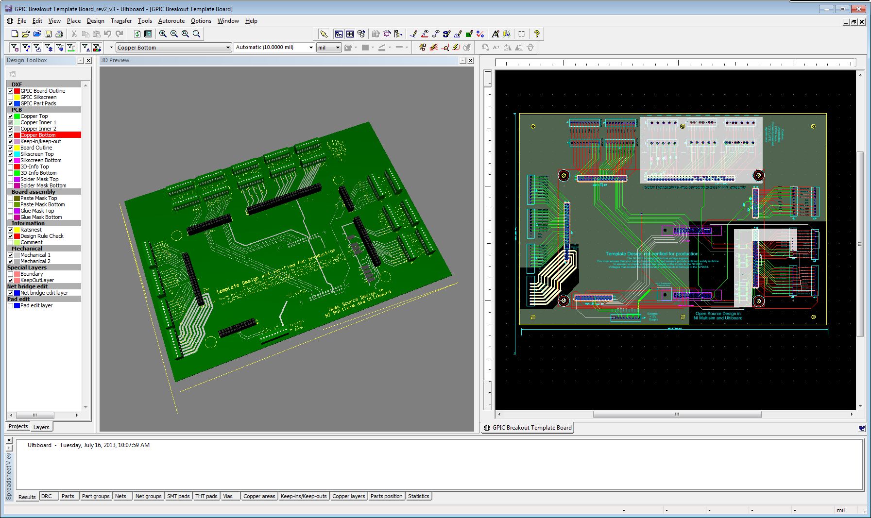
BOTTOM (Dual 26-pin connectors for SKiiP 3 and Smart PowerStack):
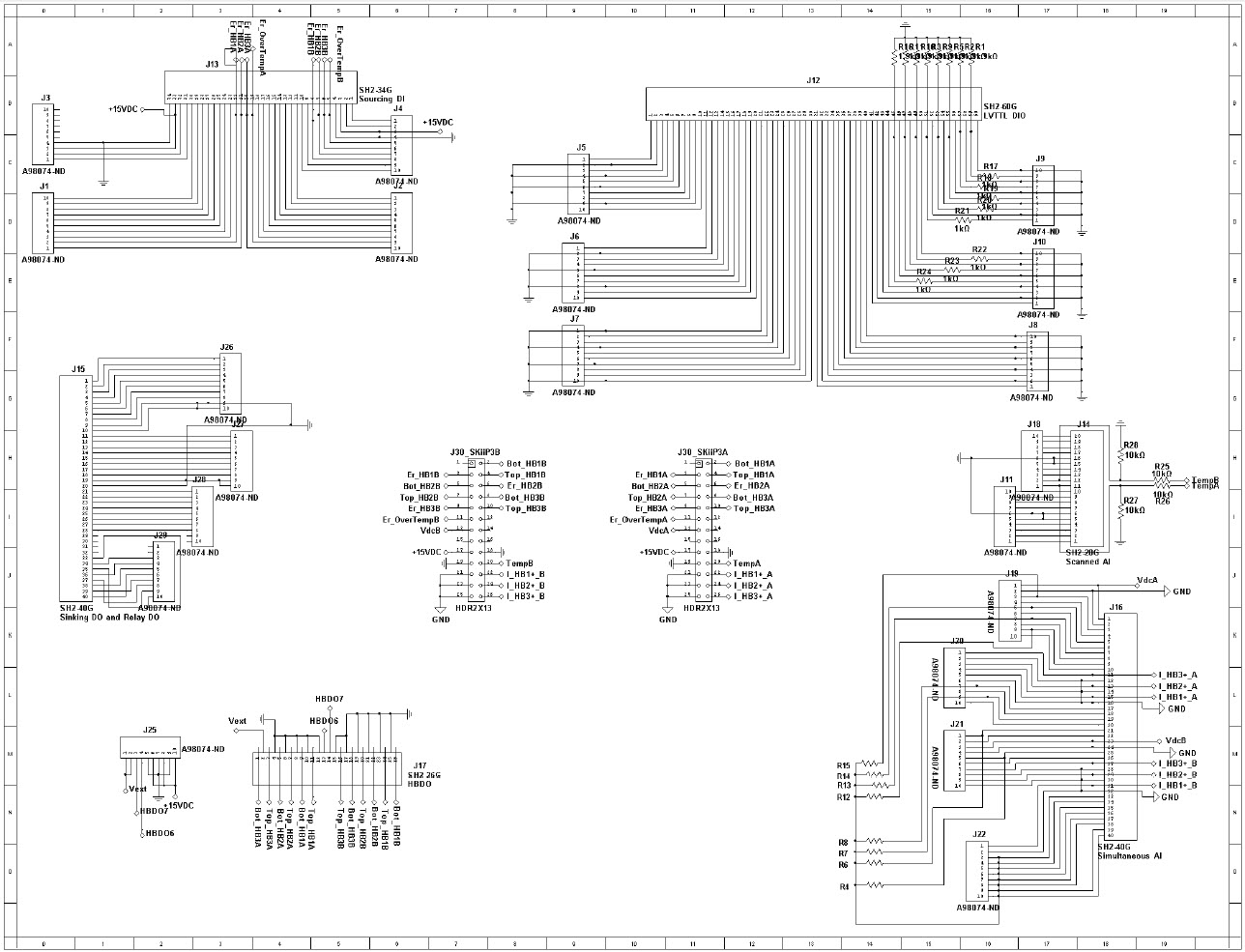
Multisim circuit schematic:
10-29-2013 10:31 AM
- Mark as New
- Bookmark
- Subscribe
- Mute
- Subscribe to RSS Feed
- Permalink
- Report to a Moderator
Is it possible to acquire one of these sample mating boards as I do no have the capacity to manufacture one myself but could really use one for a prototype project I'm starting with the 9606/9683 combination boards?
You bet. Just open the design in NI Ultiboard, export the Gerber files, and send them along with the bill of materials to a PCB/assembly house.
If you or a technician plan to solder the components on yourself, Sunstone Circuits is a good choice. The last order we placed with them was for the latest version (revision 2, version v03) using order number "FP0326871". If you reference that order number, you could call them and reorder it. Then you would purchase the screw terminal connectors and resistors from Mouser or Digikey. The IDC mating connectors for the GPIC are ordered from On-Shore (wkorbin@on-shore.com). (See the bill of materials.)
Alternately, if you want to buy a full assembled board with all the parts soldered on, either Screaming Circuits or SVTRONICS are good choices. If you are located internationally, you may wish to order from a local PCB or turnkey assembly house.
03-05-2014 11:34 AM
- Mark as New
- Bookmark
- Subscribe
- Mute
- Subscribe to RSS Feed
- Permalink
- Report to a Moderator
March 5, 2014: We are in the process of updating the GPIC Interface Board template design. In the mean time, if you are starting a new design or planning to order a board, please contact Brian MacCleery for details (brian.maccleery@ni.com).
06-27-2014 05:51 AM
- Mark as New
- Bookmark
- Subscribe
- Mute
- Subscribe to RSS Feed
- Permalink
- Report to a Moderator
Was the update published somewhere else or is it yet to be published?
07-09-2014 12:07 PM
- Mark as New
- Bookmark
- Subscribe
- Mute
- Subscribe to RSS Feed
- Permalink
- Report to a Moderator
We received PCBs two weeks ago and are currently testing the latest version. We expect to finish testing and post the updated design files within 1-2 weeks. Meanwhile, if you would like the latest design files, just email me (brian.maccleery@ni.com).
By the way, always be sure to request >= 93 mil PCB thickness for all GPIC mating boards for mechanical strength reasons.
When we post the updated design files we will also send them to SVTronics so you can order the boards from them. When ordering GPIC interface boards from SVTronics, always communicate with Angela Dodd.
Angela Dodd
Tel: 214.440.1234 x110
Cell: 972-814-1485
Fax: 214.440.1222
3465 Technology
Plano, TX. 75074
10-10-2015 08:34 AM
- Mark as New
- Bookmark
- Subscribe
- Mute
- Subscribe to RSS Feed
- Permalink
- Report to a Moderator
With a correctly designed GPIC interface PCB and proper cabinet cable routing and shielding, examples of the EMC and surge compliance tests commonly passed by sbRIO GPIC converter cabinets are listed below. These compliance tests commonly include ESD, EFT, surge, radiated, ring wave, conducted immunity, etc.
Thank you to our customer for allowing me to share these details from their test report. Below are examples of CE Compliance EMC, transient, surge tests passed by the NI sbRIO-9606 Rev. E and NI 9683 GPIC in a 100 kVA 3-phase AC (422-528 VAC, 136 A) and 550-770 VDC, 200 A DC energy storage converter cabinet:
The system passed all the tests.
The system was measured for pre-compliance with European Standards EN 61000-6-4, "Electromagnetic Compatibility (EMC) – Part 6-4: Generic Standards – Emission Standard for Industrial Environments (2007)," and IEC TS 61000-6-5, "Electromagnetic Compatibility (EMC) – Part 6-5: Generic Standards – Immunity for Power Station and Substation Environments (2001)."
Radiated emission measurement equipment and procedures were in accordance with EN 55011, "Industrial, Scientific and Medical Radio Frequency Equipment – Electromagnetic Disturbance Characteristics – Limits and Methods of Measurement (2010)." The emissions tests described in this report are used for verification with the Code of Federal Regulations Chapter 47, "Part 15 – Radio Frequency Devices, Subpart B: Unintentional Radiators," paragraph 15.107, Conducted Emission Limits and paragraph 15.109, Radiated Emission Limits. Additionally, the tests are used to show compliance with ICES-003, Issue 5 "Information Technology Equipment (ITE) – Limits and Methods of Measurement (2012)."
Immunity measurement equipment and procedures were in accordance with:
• EN 61000-4-2, "Electromagnetic Compatibility (EMC) Part 4-2: Testing and Measurement Techniques – Electrostatic Discharge Immunity Test (2009),"
• EN 61000-4-3, "EMC Part 4-3: Testing and Measurement Techniques – Radiated, Radio-Frequency, Electromagnetic Field Immunity Test (2010),"
• EN 61000-4-4, "EMC Part 4-4: Testing and Measurement Techniques – Electrical Fast Transient/Burst Immunity Test (2012),"
• EN 61000-4-5, "EMC Part 4-5: Testing and Measurement Techniques – Surge Immunity Test (2006),"
• EN 61000-4-6, "EMC Part 4-6: Testing and Measurement Techniques – Immunity to Conducted Disturbances, Induced by Radio-Frequency Fields (2009),"
• IEC 61000-4-12, "EMC Part 4-12: Testing and Measurement Techniques – Ring Wave Immunity Test (2006)."
Per the EMC test plan: For emissions, the system is Class A, Group 1 equipment. Immunity requirements and performance criteria are from EN 61000-6-5, Table 1, "Immunity Specifications – Enclosure Ports," Table 3, "Immunity Specifications – Low-voltage AC Input Power Ports and Low voltage AC Output Power Ports," and Table 4, "Immunity Specifications – Low-voltage DC Input Power Ports and Low-voltage DC Output Power Ports." There are DC input lines and AC output/control/transformer lines. There are not any possible magnetically sensitive components.
The system is compliant with the EN 61000-6-4 radiated and conducted emissions limits. The system complies when subjected to EN 61000-6-5 levels for ESD, EFT, surge, radiated, ring wave, and conducted immunity.
Section X compares the unit radiated emissions to the applicable limit from 30 MHz to 1000 MHz in accordance with equations identified in VI and the output identified in measurement procedure VIII-1. Section XI compares the unit conducted emissions to the applicable limits from 150 kHz to 30 MHz in accordance with measurement procedure VIII-2. Sections XII through XVII reference measurement procedures of VIII-3 through -8 in accordance with susceptibility and performance criteria described in Section V for type acceptance and per the manufacturer's test plan.
1. 4-kV electrical fast transients, delivered in 5-kHz bursts to the DC power lines
2. 2-kV electrical fast transients, delivered in 5-kHz bursts to the AC lines
3. 2-kV line-to-line/4-kV line-to-ground, 1.2/50microsecond combination wave surges, delivered directly or by phase synchronization to the DC input
4. 2-kV line-to-line/4-kV line-to-ground, 1.2/50microsecond combination wave surges, delivered directly or by phase synchronization to the AC lines
5. 1-kV line-to-line/2.5-kV line-to-ground, 1 MHz ring wave wave surges, delivered directly or by phase synchronization to the DC input
6. 0.5-kV line-to-line/1-kV line-to-ground, 1.2/50microsecond combination wave surges, delivered directly or by phase synchronization to the AC lines
03-09-2016 03:53 AM
- Mark as New
- Bookmark
- Subscribe
- Mute
- Subscribe to RSS Feed
- Permalink
- Report to a Moderator
Do you have the information about GPIC Interface Board (mating board) Maximum load? What is the maximum rating of load that can be driven from this board (single phase as well as three phase)?
Kind regards,
Andrej Korošec
