From Friday, April 19th (11:00 PM CDT) through Saturday, April 20th (2:00 PM CDT), 2024, ni.com will undergo system upgrades that may result in temporary service interruption.
We appreciate your patience as we improve our online experience.
From Friday, April 19th (11:00 PM CDT) through Saturday, April 20th (2:00 PM CDT), 2024, ni.com will undergo system upgrades that may result in temporary service interruption.
We appreciate your patience as we improve our online experience.
11-19-2020 12:45 PM - edited 12-28-2023 06:27 PM
The idea behind this design is to create an open source platform that allows design engineers to simulate, prototype, and deploy their Mega Watt (MW) systems at a mini-scale. This is a standard process with high power transmission and distribution systems.
The fact that the design is open source (done in Multisim and Ultiboard) enables designers to customize it as needed and develop a library of different configurations.
The design files are available to all users as a starting point. You can download the attached files from the bottom of this page, or the complete power electronics design guide LabVIEW project. You can configure the FPGA control code, customize the analog front-end of the system, and recreate your own version of the design.
Examples of applications that could be modeled using this design are:
A major contributor to the effectiveness of this design is the accurate system desktop co-simulation prior to prototyping. LabVIEW FPGA and Multisim offer a variable time step co-simulation functionality of the complete system made of the analog plant (including the IGBTs, RLC filter output stage, bridge rectifiers, and precharge contactors) and the FPGA control code (including RMS/phase calculation, PLL blocks, PWM generation). The power inverter co-simulation code is available in the power electronics design guide.
Co-simulation of this system showed excellent agreement with the acquired measurements from the system prototype. However it helped evaluate the following performance parameters before prototyping which lead to a single prototype spin to get to the final working hardware design:
The design topology contains two power inverters in back-to-back configuration to support the different application use-cases previously mentioned. A single FPGA-based controller is compiled on the sbRIO-9606 and the connectivity to the inverters is implemented through the NI GPIC. This section provides explanation of the circuitry in each of the blocks of the block diagram shown below.
These sub-circuits include two 3-phase inverter chips and two bridge rectifiers. Each chip is a 6-pack intelligent power module (IPMs) with built in gate-drivers and thermistor temperature sensing from ST Microelectronics (STGIPS10K60A). The design includes all the recommended decoupling capacitance. Operation is tested with control loops up to 20kHz.
The board operation is rated at 50VDC and 8A of current and the DC link includes in-rush current control using a thermistor and a relay contactor controlled using the GPIC.
Also included in the design is on board current and voltage sensors for each half-bridge. The hall-effect sensors ASC712 from Allegro are used to sample the currents while the voltages are sampled using potential dividers. All the sensed signals range between +10V and -10V and are routed to the isolated simultaneous analog inputs of the GPIC.
These sub-circuits include the necessary electronics to maintain isolation between the controller digital section, and the inverter analog section of the design.
The switching command signals (S1A, S1B, S2A, S2B…, S6A, S6B) coming from the GPIC are responsible for toggling the IGBTs inside the 6-pack IPM. These signals are first isolated using opto-couplers before getting to the power side.
All the current sensors are powered using an isolated buck converter supply (VBT1-S12-S12).
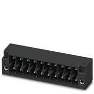
This sub-circuit includes the entire break-out connectors to the GPIC signals. Right-angled headers with pluggable terminal blocks from Phoenix connectors were chosen to make an easy wire-poke connection.
All the connections to the GPIC I/O pass through jumpers that have to be physically placed at the bottom of the board. This feature is helpful in case these I/O lines need to be used in some other way.
Also 8 of the +3.3V LVTTL DIO lines are connected to on-board potential dividers in case +5V digital input lines need to be connected to directly to the board (for example, signals from a motor speed encoder)


Two supplies are needed to power up the board:
The analog plant circuitry is prototyped on a custom PCB in Ultiboard. The design maintains complete isolation between the high-power analog signals and the low power digital control signals. To do so, the board is comprised of three main sections:
For more details on the FPGA controller of this design and the overall system performance, refer to this page.