From Friday, April 19th (11:00 PM CDT) through Saturday, April 20th (2:00 PM CDT), 2024, ni.com will undergo system upgrades that may result in temporary service interruption.
We appreciate your patience as we improve our online experience.
From Friday, April 19th (11:00 PM CDT) through Saturday, April 20th (2:00 PM CDT), 2024, ni.com will undergo system upgrades that may result in temporary service interruption.
We appreciate your patience as we improve our online experience.
08-31-2017 05:48 PM
Hi,
I read some literature on using FPGA to implement time-to-digital converter (TDC) for fluorescence lifetime imaging. There are some FPGA example code online but are mostly written in VHDL or Verilog. I noticed that NI PXIe-7972R FPGA has TDC IO available, but couldn't find any documentation about it. Can anyone please share a simple example or some experience on how to use the TDC IO?
Thanks,
Bing
Solved! Go to Solution.
09-01-2017 01:23 PM - edited 09-01-2017 01:29 PM
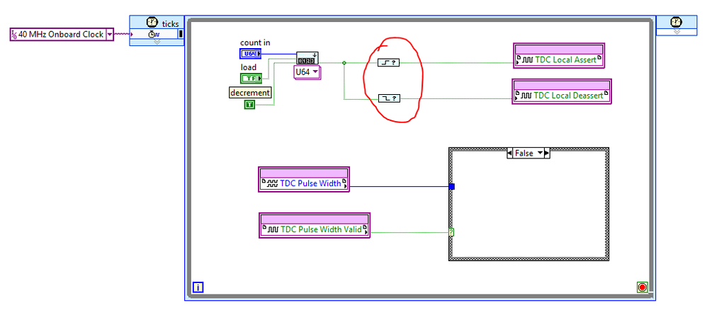
The TDC exposed on the 797x targets is a pulse expander. So toggle the assert then the deassert. The pulse expanding circuitry will then apply some expansion factor to the time duration between assert-deassert and return the duration of the expanded signal width.
Pulse Width = (TimeWhenDeasserted - TimeWhenAsserted) * ExpansionFactor
So if there are 10 ticks between assertions in the 40MHz clock domain and the expansion is 10 ( i don't know what the expansion factor is, I'm guessing) you'll get a pulse width of 100. Here is an example that you can use to test the TDC. Set the number of ticks you want to wait between assertions on 'count in', then toggle 'load'.
The tricky part is calibrating the expansion factor which may change some tiny amount if the ambient temperature changes. Let me know how it goes.
09-03-2017 08:35 PM - edited 09-03-2017 08:35 PM
Dear David-A,
Thank you so much for your reply. I downloaded your example but unfortunately I'm using LabVIEW 2015 so I cannot open the project. I was able to create the FPGA vi based on your screenshot. Can you please share a screenshot of the host vi?
My another question is: it seems the TDC function only supports 40MHz onboard clock. If that is the case and the expansion is 10, does that mean the best time resolution I can get with TDC is only 2.5ns? In articles people claimed they can reach <0.1ns resolution with TDC on FPGA, do you think it is doable with NI FPGA?
Thanks,
Bing
09-06-2017 10:20 AM
Bing,
Here's a screenshot of the host. I also saved the project as 2015 version.
09-06-2017 03:46 PM - edited 09-06-2017 03:47 PM
Hi brandonj,
Thanks for your help!
I was able to run the code. If my understanding about the FPGA code is correct, what it does is to start counting down from the count in value until 0, and Count Down U64 subvi output changes from False to TRUE, triggering the rising edge detector. After another tick, the value changes back to false and is detected by the falling edge detector. The delay between the two events will be expanded by TDC circuitry and output as TDC Pulse Width. So no matter what the count in value is, the output from the Count Down subvi is always a 25ns (1/40MHz) digital pulse. If that is the case, then there are a few questions:
1. Note that in David-A's and your example code, TDC Local Assert is connected to falling edge detection while TDC Local Deassert to rising edge detection. Shouldn't it be the other way around? Nevertheless, I ran your original code and the TDC Pulse Width was always ~2400 (with some single-digit variations). I then switched the placement of rising/falling edge detectors, recompiled the code and surprisingly the result was the same as your original code.
2. To further test how TDC works, I rewrote the code by replacing the Count Down subvi with a Pulse Train Generator that output digital pulses of variable width (please see the attached screenshot below). If TDC works as I assumed, the TDC Pulse Width should change with the input pulse width. However it remained (almost) constant no matter of On/Off Time, and the result is about twice the value of the example code.
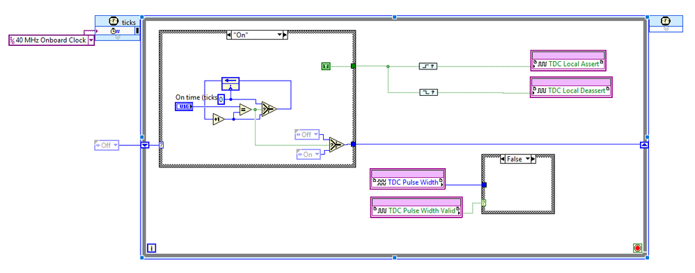
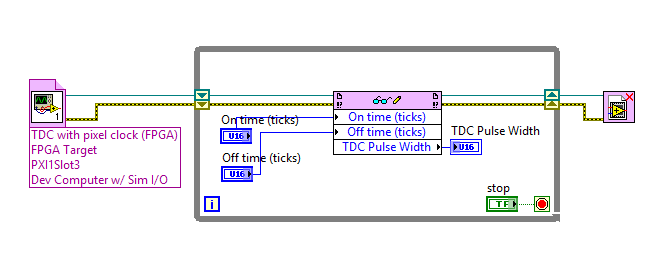
It appears TDC does not work as expected. Or did I miss anything?
Thanks,
Bing
09-07-2017 02:08 PM - edited 09-07-2017 02:16 PM
My apologies, the example I gave you incorrectly applies a single tick pulse to the TDC (as seen in the top half of the image below). What the TDC requires is an assert that remains high until a deassert is observed (seen in the lower half of the image below). The deassert should transition high before assert transitions low, it should also remain high at least two clock cycles. Doing this will help avoid avoid inducing jitter in the pulse width measurement.
Also you can use any clock domain you want for tdc assert and deassert. The pulse width and width valid must be in the 40 MHz domain though.
09-08-2017 02:36 PM
Dear David-A,
Thank you so much for your help. I modified your new example slightly and now the TDC implementation works!
For future reference, my modifications are below:
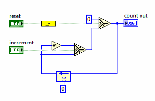
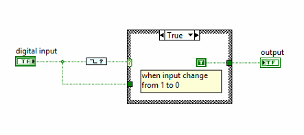
I rewrote the standard Count Up.vi by adding a rising edge detection so that assert goes high only when reset changes from false to true. And my LV2015 doesn't have Pulse Expander 2x.vi so I wrote a small vi to extend a digital pulse HIGH by 1 tick.
Now some more questions:
1. Is the original pulse width, i.e., (TimeWhenDeasserted - TimeWhenAsserted), determined by the two rising edges as shown ?
2. The equation you wrote in your original post
TDC Pulse Width = (TimeWhenDeasserted - TimeWhenAsserted) * ExpansionFactor
slightly deviates from my observation with the latest example. As shown below, assert width does have a linear correlation with TDC pulse width. I assume the slope of the fitting plot corresponds to the Expansion Factor (at 160MHz)? Somehow the plot doesn't intercept at (0,0) though. Does that mean when calculating TDC pulse width we need to consider a constant offset?
3. I am still a little uncertain about the unit of TDC pulse width. Use the data (plot) above as an example, where Assert/Deassert runs in 160MHz timed. 1 tick increment of assert width corresponds to 524.67 TDC pulse width, does that mean the time resolution of TDC at 160MHz is 1/160e6/524.67 = 11.9 ps?
4. I also tested the FPGA code at other clock frequencies (e.g., 40MHz and 280MHz) and the data is listed below. Do the values similar to what you got?
|
SCTL Clock |
Expansion Factor |
Std err |
Time resolution (ps) |
Error (ps) |
|
40 MHz |
1774.9 |
31.92 |
14.1 |
449.6 |
|
160 MHz |
524.67 |
3.62 |
11.91 |
43.17 |
|
280 MHz |
313.82 |
3.16 |
11.38 |
36.0 |
Thanks,
Bing