From 04:00 PM CDT – 08:00 PM CDT (09:00 PM UTC – 01:00 AM UTC) Tuesday, April 16, ni.com will undergo system upgrades that may result in temporary service interruption.
We appreciate your patience as we improve our online experience.
From 04:00 PM CDT – 08:00 PM CDT (09:00 PM UTC – 01:00 AM UTC) Tuesday, April 16, ni.com will undergo system upgrades that may result in temporary service interruption.
We appreciate your patience as we improve our online experience.
03-28-2013 09:37 AM
Hi,
apologize for the trivial question....
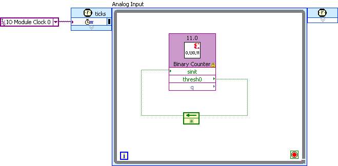
It sometimes happens to me to feed signals back as the boolean in the following diagram.
The figure below is a simplified example: a synchronous counter that, upon arriving at a given threshold,
re-initialize synchronously to a given value (and again and again). Just as an example.
When I draw this feedback wire, LV did authomatically insert a Feedback Node. This would
make perfect sense if the signal were around a combinatorial block; however here the block, a synchronous counter,
has nothing combinatorial, so the additional Feedback Node seems to me useless. Moreover,
in actual situations, it is very uncomfortable to me, as it complicates the timing.
Is there any way to remove it?
Thanks!
Bruno
03-28-2013 09:40 AM
Ooops.. here is the figure.
03-28-2013 09:45 AM
I don't think LV knows your IP block is synchronous to a given clock, so I can't imagine it'll let you remove that FN; I was taught that it treats all blocks (VIs, prims, xnodes, etc.) inside an SCTL as combinatorial logic. It seems like NI would have to make a special rule for VHDL generation that ignores the FN, since connecting an input and an output on the same block is a violation of dataflow itself.
03-28-2013 10:27 AM
David is correct in that we don't allow this because it breaks our structured dataflow syntax. We would have to create some kind of execption to allow for this in FPGA diagrams, but this presents complications for code which might be used on both the host and FPGA (e.g. host simulation of an FPGA block).
LabVIEW does know your block is synchronous to a given clock - that is actually a property of the LabVIEW FPGA diagram. This is purely a reflection of our desire to deliver a consistent dataflow syntax across targets (Windows, RT, FPGA, etc.).
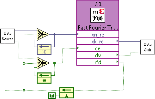
For this counter example, our recommendation would of course be to include this feedback node as part of the subVI logic. In practice, for me this is generally not an issue. The one instance where it does often arise is flow control of multi-rate blocks, in particular when using our "4-wire" protocol, where this feedback node can delay the propagation of back-pressure to upstream blocks. But even this can generally be addressed by a small about of buffer logic to filter out potential "lock-up" conditions where two or more blocks might have non-friendly behavior in terms of when they are and aren't ready for data or producing data. The real rub lies when going between Xilinx or HDL blocks and LabVIEW blocks, where such handshaking signals do not have this behavior. Generally, a 1-deep FIFO on the input to the HDL block can help to allieviate this, effectively "re-trying" input data from an upstream LabVIEW block, on cycles when the Xilinx / HDL block indicated that it wasn't ready for data (but the upstream LabVIEW block could not be aware of this because of the one-cycle delay of the feedback node). Here is an example of that logic:
Hope this helps,
Ryan
03-28-2013 11:27 AM
Just to extend on the previous comments, in general you must treat any data that may be fed upstream as a next-cycle value. The 4-wire protocol used by the streaming blocks in LabVIEW FPGA (e.g. the High-Throughput nodes) exemplify this where the Ready for Input that feeds into upstream nodes carries a value for the next cycle. That way you are able to register each of those values in the owning diagram and meet the dataflow requirements of LabVIEW.
When you are using Xilinx IP, many of the blocks can be configured to output this "next cycle" value instead of the registered synchronous version. If not, then unfortunately you have to do the work to support the extra cycle of latency.
03-28-2013 01:03 PM
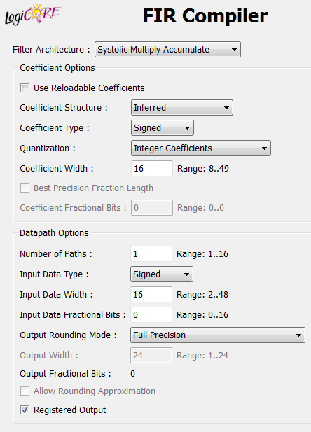
Wow... I've never considered that, but it makes total sense. I always thought that registering the outputs of the Xilinx cores did not change the behavior of the signals at the port map (which would require additional "anticipation" when registering the RFD). But if it is truly just a register, then I suppose we can avoid the caching registers shown in my code above. For instance, in the FIR Compiler, does the "Registered Output" checkbox also control RFD behavior?
I generally register outputs to avoid timing issues, but there is no reason I couldn't register the data outputs (but not RFD) with feedforward nodes on the LabVIEW diagram. That would be a whole lot easier than the caching logic.
Thanks for the tip!
Ryan
03-28-2013 02:28 PM
In your example Ryan, if you uncheck "Registered Output", then the Ready signals should also be unregistered (or just an earlier "next cycle" calculation) so they remain aligned. If that is not the case, I'd love to see what Xilinx does to the interface to properly handle the data.
03-28-2013 03:12 PM
Hi Dragis,
Unfortunately it appears that this is not the case for the FIR core. In the timing diagram below, with outputs registered, RFD goes low the next clock cycle after valid data is presented at the data inputs:
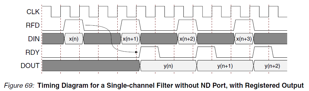
with outputs unregistered, the behavior is identical:
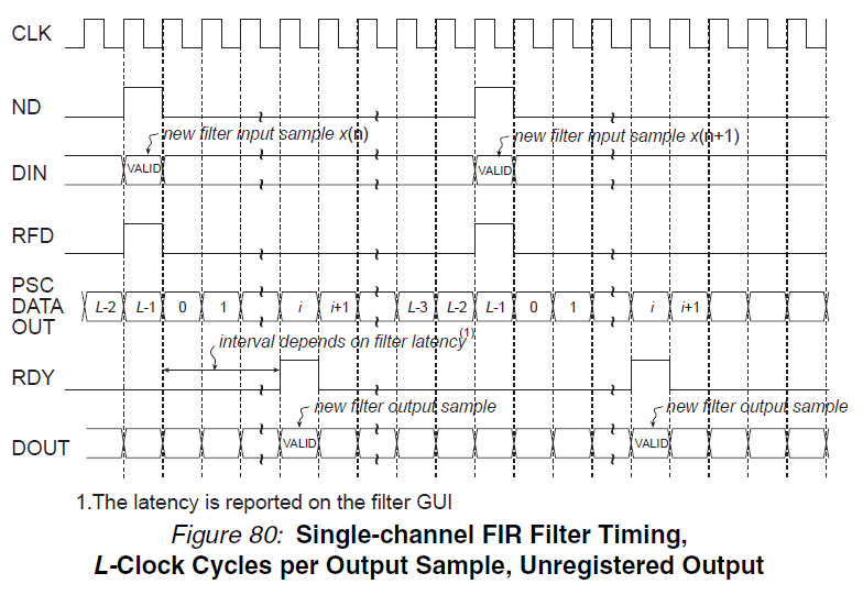
The RFD signal does not come any sooner, which would be implied if the signal were simply registered in one case, and not in the other. Thinking about it a bit more, this actually makes perfect sense, since RFD is dependent upon the presence of (previously) valid data on the input ports, and does not directly depend on the data at the output port. This isn't the case for the RDY signal, however, (which appears to be registered), which should go high when new data is present on the output port.
I'm afraid the caching logic on the input might be necessary if this behavior is shared across Xilinx cores.
Ryan
03-28-2013 03:18 PM
Yeah, that makes sense. The core would have to specify that you want the next cycle values for the input data logic.
