- Subscribe to RSS Feed
- Mark Topic as New
- Mark Topic as Read
- Float this Topic for Current User
- Bookmark
- Subscribe
- Mute
- Printer Friendly Page
Creating FPGA Testbenches involving DMAs?
09-24-2012 01:09 PM
- Mark as New
- Bookmark
- Subscribe
- Mute
- Subscribe to RSS Feed
- Permalink
- Report to a Moderator
Hello all,
I'm working on a project that utilizes multiple PXIe-7962Rs in communication with a LabVIEW RT host. I'm using DMA FIFOs for
communication between the FlexRIOs and the host, and I would like to create a testbench vi to send simulated data transfers over
the DMA FIFOs, to check the functionality of my address decoder and other logic. I started with this tutorial:
http://zone.ni.com/reference/en-XX/help/371599G-01/lvfpgaconcepts/test_bench_tutorial/
But it only covers FPGA I/O nodes, which I'm actually not currently using in my project. My specific problem is this: I tried entering the resource name of
one of my DMA FIFO's as an option in the outer "I/O Item Name Case Structure," but the enumerated choices wired from subVI 3 to the selector terminal of the inner structure, "Node or Element Type Case Structure," appear to be hard-coded to the two methods for the FPGA I/O node, "I/O read" and "I/O write." I want
a way to return a simulated value when my FPGA vi checks, say, the number of items in the DMA FIFO, or does a read from it.
Is this possible? If so, how do I determine the proper resource names and resource method names to invoke? I would be grateful for any suggestions.
09-24-2012 01:46 PM
- Mark as New
- Bookmark
- Subscribe
- Mute
- Subscribe to RSS Feed
- Permalink
- Report to a Moderator
Without knowing your testbench hierarchy - here's what I would suggest doing in your testbench VI. I do everything using modelsim as my 3rd party simulator, and this works for simulating IO from a 'host' VI to the FPGA.
1) Open a reference to your FPGA personality. (fpga interface pallette -> open)
2) use "read/write control" (fpga interface pallette -> read/write control) node to handle host control/status to/from controls/indicators on your FPGA. Wire your FPGA reference into that node. Then the node will allow you to select controls/indicators to read/write. Use this to do any setup and configuration you might need.
3) use "invoke method" (fpga interface pallette -> invoke method ). When you select the method - you can choose your FIFO, and then choose to read or write from it.
4) Configure the read or write FIFO block on your diagram for the number of elements to read or write (a 0-element read or write will simply return the number of elements to read or to write, respectively). The input to the DMA Write block is an array of values which will be sent serially to your device. Data output from a DMA read will be an array.
-Jim
09-24-2012 02:37 PM
- Mark as New
- Bookmark
- Subscribe
- Mute
- Subscribe to RSS Feed
- Permalink
- Report to a Moderator
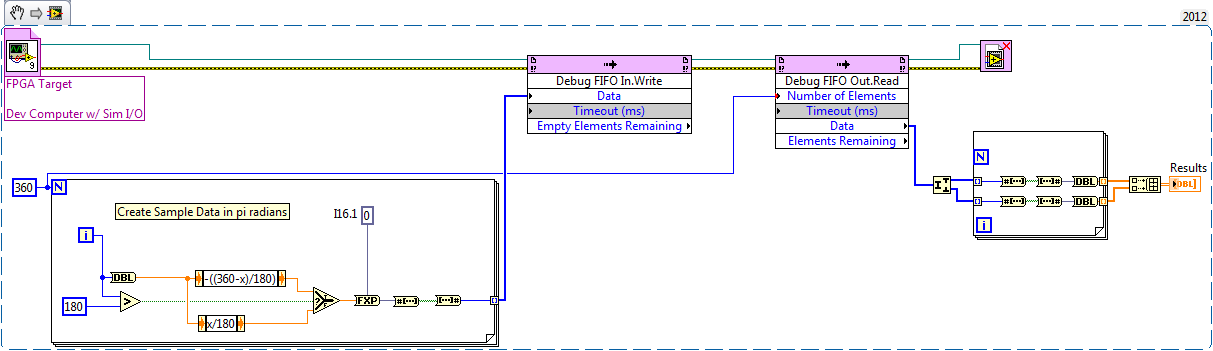
Here are some graphical images for what Jim is talking about. The FPGA does a simple sin/cos calculation (the FIFO Read/Write subVIs are available in the FlexRIO Development Tools download).
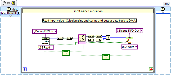
The host sends input data through the DMA fifo using an Invoke Method in the FPGA Interface palette (right-click a non-FPGA context block diagram»FPGA Interface). The correct input DMA FIFO is selected and another Invoke Method pointed at the output FIFO waits on return data.
Some general tips:
- Use the Timed Out? indicator and a case structure in your FPGA to handshake FIFO reads and writes with upstream/downstream logic. This will prevent incorrect results due to overflow or underflow
- Bitpack data to maximize throughput. In this example, I pack the 2 I16 results into a single U32; it saves me an extra FIFO. For debugging, you can pack similar logic into a single integer, like boolean status lines or smaller width result values.
09-24-2012 08:35 PM
- Mark as New
- Bookmark
- Subscribe
- Mute
- Subscribe to RSS Feed
- Permalink
- Report to a Moderator
Thanks,
I followed your suggestions and it worked like a charm. If I could ask some follow-up:
1. If I have two FlexRIO devices, and vi's targeted for each that are both set to run on the development computer, should I be able to follow a similar approach to what you just suggested
to set up and send data over a simulated peer-to-peer stream between them?
2. If I'm using socketed or unsocketed CLIP, should I be able to simulate input and output for the CLIP IO using the approach described in the tutorial in my first post in this thread?
3. If I am using Xilinx Coregen IP nodes or IP imported with the IP integration node, will they have functionally-equivalent (I know for sure not timing equivalent) behavior when I run the vi on the
dev computer, or do I need to cosimulate with Modelsim or export to ISim to include these IP nodes in a simulation?
09-25-2012 01:19 PM
- Mark as New
- Bookmark
- Subscribe
- Mute
- Subscribe to RSS Feed
- Permalink
- Report to a Moderator
1. If I have two FlexRIO devices, and vi's targeted for each that are both set to run on the development computer, should I be able to follow a similar approach to what you just suggested
to set up and send data over a simulated peer-to-peer stream between them?
If I were simulating P2P streaming, you could do this with 2 DMA fifos: Read chunks of data from one FlexRIO and call the Write method for the other. I would definitely make sure that you have handshaking for the FIFOs in your FPGA code, as the latency of the simulation will be affected.
2. If I'm using socketed or unsocketed CLIP, should I be able to simulate input and output for the CLIP IO using the approach described in the tutorial in my first post in this thread?
You could use that method, but I really never have. You can simulate CLIP I/O either with by using a DMA FIFO with data from the host, or you can use FPGA memories to output simulated waveforms.
3. If I am using Xilinx Coregen IP nodes or IP imported with the IP integration node, will they have functionally-equivalent (I know for sure not timing equivalent) behavior when I run the vi on the
dev computer, or do I need to cosimulate with Modelsim or export to ISim to include these IP nodes in a simulation?
The IP Integration node and Coregen IP should functionally behave correctly in simulation; the node builds a simulation DLL that allows it to provide data when Development Computer is selected. You shouldn't have to use Modelsim or ISim, although I would to verify timing before you do a compile.
