-
NI Community
- Welcome & Announcements
-
Discussion Forums
- Most Active Software Boards
- Most Active Hardware Boards
-
Additional NI Product Boards
- Academic Hardware Products (myDAQ, myRIO)
- Automotive and Embedded Networks
- DAQExpress
- DASYLab
- Digital Multimeters (DMMs) and Precision DC Sources
- Driver Development Kit (DDK)
- Dynamic Signal Acquisition
- FOUNDATION Fieldbus
- High-Speed Digitizers
- Industrial Communications
- IF-RIO
- LabVIEW Communications System Design Suite
- LabVIEW Electrical Power Toolkit
- LabVIEW Embedded
- LabVIEW for LEGO MINDSTORMS and LabVIEW for Education
- LabVIEW MathScript RT Module
- LabVIEW Web UI Builder and Data Dashboard
- MATRIXx
- Hobbyist Toolkit
- Measure
- NI Package Manager (NIPM)
- Phase Matrix Products
- RF Measurement Devices
- SignalExpress
- Signal Generators
- Switch Hardware and Software
- USRP Software Radio
- NI ELVIS
- VeriStand
- NI VideoMASTER and NI AudioMASTER
- VirtualBench
- Volume License Manager and Automated Software Installation
- VXI and VME
- Wireless Sensor Networks
- PAtools
- Special Interest Boards
- Community Documents
- Example Programs
-
User Groups
-
Local User Groups (LUGs)
- Denver - ALARM
- Bay Area LabVIEW User Group
- British Columbia LabVIEW User Group Community
- Chicago LabVIEW User Group
- Egypt NI Chapter
- GUNS
- Houston Area LabVIEW Community
- LabVIEW - University of Applied Sciences Esslingen
- [IDLE] LabVIEW User Group Stuttgart
- LUGG - LabVIEW User Group at Goddard
- LUGNuts: LabVIEW User Group for Connecticut
- Madison LabVIEW User Group Community
- Mass Compilers
- Melbourne LabVIEW User Group
- Midlands LabVIEW User Group
- Milwaukee LabVIEW Community
- Minneapolis LabVIEW User Group
- CSLUG - Central South LabVIEW User Group (UK)
- Nebraska LabVIEW User Community
- New Zealand LabVIEW Users Group
- NI UK and Ireland LabVIEW User Group
- NOCLUG
- Orange County LabVIEW Community
- Ottawa and Montréal LabVIEW User Community
- Washington Community Group
- Phoenix LabVIEW User Group (PLUG)
- Politechnika Warszawska
- PolŚl
- Rutherford Appleton Laboratory
- Sacramento Area LabVIEW User Group
- San Diego LabVIEW Users
- Sheffield LabVIEW User Group
- South East Michigan LabVIEW User Group
- Stockholm LabVIEW User Group (STHLUG)
- Southern Ontario LabVIEW User Group Community
- SoWLUG (UK)
- Space Coast Area LabVIEW User Group
- Sydney User Group
- Top of Utah LabVIEW User Group
- Utahns Using TestStand (UUT)
- UVLabVIEW
- Western NY LabVIEW User Group
- Western PA LabVIEW Users
- Orlando LabVIEW User Group
- Aberdeen LabVIEW User Group (Maryland)
- Gainesville LabVIEW User Group
- LabVIEW Team Indonesia
- Ireland LabVIEW User Group Community
- Louisville KY LabView User Group
- NWUKLUG
- LVUG Hamburg
- LabVIEW User Group Munich
- LUGE - Rhône-Alpes et plus loin
- London LabVIEW User Group
- VeriStand: Romania Team
- DutLUG - Dutch LabVIEW Usergroup
- WaFL - Salt Lake City Utah USA
- Highland Rim LabVIEW User Group
- NOBLUG - North Of Britain LabVIEW User Group
- North Oakland County LabVIEW User Group
- Oregon LabVIEW User Group
- WUELUG - Würzburg LabVIEW User Group (DE)
- LabVIEW User Group Euregio
- Silesian LabVIEW User Group (PL)
- Indian LabVIEW Users Group (IndLUG)
- West Sweden LabVIEW User Group
- Advanced LabVIEW User Group Denmark
- Automated T&M User Group Denmark
- UKTAG – UK Test Automation Group
- Budapest LabVIEW User Group (BudLUG)
- South Sweden LabVIEW User Group
- GLA Summit - For all LabVIEW and TestStand Enthusiasts!
- Bangalore LUG (BlrLUG)
- Chennai LUG (CHNLUG)
- Hyderabad LUG (HydLUG)
- LUG of Kolkata & East India (EastLUG)
- Delhi NCR (NCRLUG)
- Montreal/Quebec LabVIEW User Group Community - QLUG
- Zero Mile LUG of Nagpur (ZMLUG)
- LabVIEW LATAM
- LabVIEW User Group Berlin
- WPAFB NI User Group
- Rhein-Main Local User Group (RMLUG)
- Huntsville Alabama LabVIEW User Group
- LabVIEW Vietnam
- [IDLE] ALVIN
- [IDLE] Barcelona LabVIEW Academic User Group
- [IDLE] The Boston LabVIEW User Group Community
- [IDLE] Brazil User Group
- [IDLE] Calgary LabVIEW User Group Community
- [IDLE] CLUG : Cambridge LabVIEW User Group (UK)
- [IDLE] CLUG - Charlotte LabVIEW User Group
- [IDLE] Central Texas LabVIEW User Community
- [IDLE] Cowtown G Slingers - Fort Worth LabVIEW User Group
- [IDLE] Dallas User Group Community
- [IDLE] Grupo de Usuarios LabVIEW - Chile
- [IDLE] Indianapolis User Group
- [IDLE] Israel LabVIEW User Group
- [IDLE] LA LabVIEW User Group
- [IDLE] LabVIEW User Group Kaernten
- [IDLE] LabVIEW User Group Steiermark
- [IDLE] தமிழினி
- Academic & University Groups
-
Special Interest Groups
- Actor Framework
- Biomedical User Group
- Certified LabVIEW Architects (CLAs)
- DIY LabVIEW Crew
- LabVIEW APIs
- LabVIEW Champions
- LabVIEW Development Best Practices
- LabVIEW Web Development
- NI Labs
- NI Linux Real-Time
- NI Tools Network Developer Center
- UI Interest Group
- VI Analyzer Enthusiasts
- [Archive] Multisim Custom Simulation Analyses and Instruments
- [Archive] NI Circuit Design Community
- [Archive] NI VeriStand Add-Ons
- [Archive] Reference Design Portal
- [Archive] Volume License Agreement Community
- 3D Vision
- Continuous Integration
- G#
- GDS(Goop Development Suite)
- GPU Computing
- Hardware Developers Community - NI sbRIO & SOM
- JKI State Machine Objects
- LabVIEW Architects Forum
- LabVIEW Channel Wires
- LabVIEW Cloud Toolkits
- Linux Users
- Unit Testing Group
- Distributed Control & Automation Framework (DCAF)
- User Group Resource Center
- User Group Advisory Council
- LabVIEW FPGA Developer Center
- AR Drone Toolkit for LabVIEW - LVH
- Driver Development Kit (DDK) Programmers
- Hidden Gems in vi.lib
- myRIO Balancing Robot
- ROS for LabVIEW(TM) Software
- LabVIEW Project Providers
- Power Electronics Development Center
- LabVIEW Digest Programming Challenges
- Python and NI
- LabVIEW Automotive Ethernet
- NI Web Technology Lead User Group
- QControl Enthusiasts
- Lab Software
- User Group Lead Network
- CMC Driver Framework
- JDP Science Tools
- LabVIEW in Finance
- Nonlinear Fitting
- Git User Group
- Test System Security
- Product Groups
- Partner Groups
-
Local User Groups (LUGs)
-
Idea Exchange
- Data Acquisition Idea Exchange
- DIAdem Idea Exchange
- LabVIEW Idea Exchange
- LabVIEW FPGA Idea Exchange
- LabVIEW Real-Time Idea Exchange
- LabWindows/CVI Idea Exchange
- Multisim and Ultiboard Idea Exchange
- NI Measurement Studio Idea Exchange
- NI Package Management Idea Exchange
- NI TestStand Idea Exchange
- PXI and Instrumentation Idea Exchange
- Vision Idea Exchange
- Additional NI Software Idea Exchange
- Blogs
- Events & Competitions
- Optimal+
- Regional Communities
- NI Partner Hub
-
 bikeron
on:
New International Rectifier Components in Multisim 14.0
bikeron
on:
New International Rectifier Components in Multisim 14.0
-
 giondoo77
on:
Creating Custom Arduino Shields With NI Multisim
giondoo77
on:
Creating Custom Arduino Shields With NI Multisim
- robo_Jeff on: Multisim Touch for iPad Now Available
-
doa4378
on:
New Models for Photovoltaic Cells in Multisim
- Mahmoud_W on: Connectors for NI 78xxR Multifunction RIO series in Multisim
- Mahmoud_W on: Search for Components in Digi-Key's Database While Building Your Circuit in Multisim
-
 BMac
on:
Ultiboard Mating PCB Design of the new NI GPIC Platform for Energy Applications
BMac
on:
Ultiboard Mating PCB Design of the new NI GPIC Platform for Energy Applications
-
Henry_Lavery
on:
Automotive Application: Hall Effect Sensor in Multisim
- GarretF on: LabVIEW-Multisim Co-Simulation with Variants and Hierarchical Blocks (Part 2)
-
Control_Dir
on:
Adding 3D Information in Ultiboard
PCB Transmission Line Calculator in Ultiboard
- Subscribe to RSS Feed
- Mark as New
- Mark as Read
- Bookmark
- Subscribe
- Printer Friendly Page
- Report to a Moderator
Hello Circuit Designers,
When creating PCB layouts, many routing aspects that may not be accounted for in the SPICE simulation should be accounted for. One of the most critical routing parameters affecting the quality of the signals on the PCB is impedance matching.
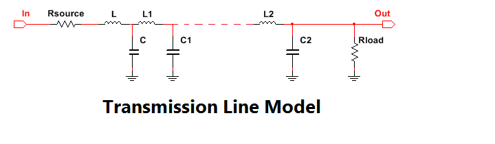
For low-frequency analog signals impedance matching is easy to achieve using simple buffer stages with high input impedance and low output impedance to maximize the power transfer at each stage of the design. However, when the frequency of the analog signal gets to the Mega-Hertz range, the PCB trace itself becomes a transmission line of a distributor nature. In simple words, the trace acts like a chain of series inductors and parallel capacitors. These elements are able to store energy and reflect it back unless the termination is a load resistance equal to the characteristic impedance of that transmission line (calculated by the below equation).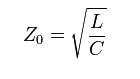 The same concept applies to all digital signals since they have an infinte span in the frequency domain.
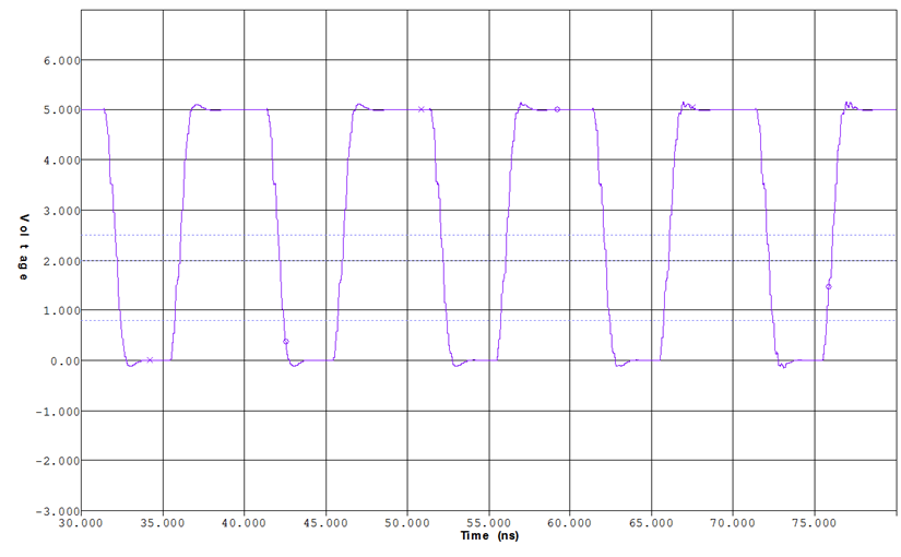
The following two graphs display a 5V digital logic signal propagating through a 50-ohm transmission line. In the first graph the line is open-ended, the second case the line is terminated with a 42-ohm load (close to perfectly matched).
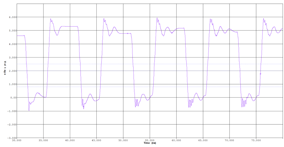
As you can see on the first graph, the reflection on the open-ended line caused a ripple of about 1V on the signal level which could propate back into the circuit and damage it.
To be able to create matched traces and avoid undesired reflections on the PCB, you need to answer these questions:
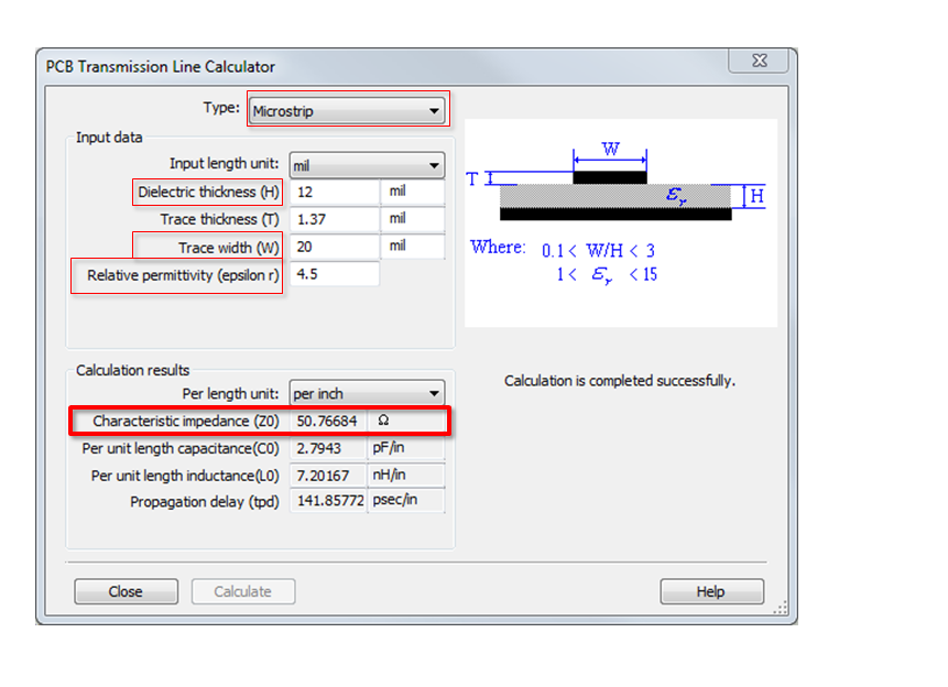
1. How thick is the PCB and what dielectric material is it made of?
2. What is the impedance of the load? (50 or 75 ohms in most of the cases)
Using these parameters, Ultiboard's transmission line calculator can help you determine the optimum width of the traces you are about to lay down on your board. Simply go to Tools>PCB transmission line calculator in Ultiboard's menu and enter these parameters as shown in the screenshot below.
(Note: choose the type of the transmission line based on where the trace the ground plane are. For example, pick Microstrip if the trace is on the top layer and the ground plane is on the first copper inner layer. In this case the board thickness will be the height (H) between these two layers)
Mahmoud W
National Instruments
You must be a registered user to add a comment. If you've already registered, sign in. Otherwise, register and sign in.
