- Subscribe to RSS Feed
- Mark Topic as New
- Mark Topic as Read
- Float this Topic for Current User
- Bookmark
- Subscribe
- Mute
- Printer Friendly Page
Cant figure out the 74LS09D and gate
02-04-2020 12:48 AM
- Mark as New
- Bookmark
- Subscribe
- Mute
- Subscribe to RSS Feed
- Permalink
- Report to a Moderator
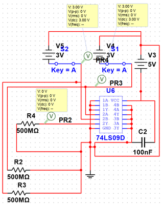
I have been trying to use this and gate in a circuit, and I couldnt get it working. I then made an isolated and gate circuit but still couldnt get any output to be high. Here is a photo of my circuit in action. Both inputs high, output low. Can someone please explain where I am going wrong?
04-11-2020 04:10 AM
- Mark as New
- Bookmark
- Subscribe
- Mute
- Subscribe to RSS Feed
- Permalink
- Report to a Moderator
There are two main problems in your circuit. First, at the output of the AND gate. Second, at the input terminals of the AND gate.
To recognize the first problem, we need to understand the nature of the output stage of the logic device used in the circuit. The 74LS09 is a quadruple two-input AND gate with OPEN-COLLECTOR output. What prevents your circuit from functioning properly is the OPEN-COLLECTOR output.
The usual output structure of bipolar TTL gates, which the 74LS (low-power Schottky) family belongs, uses the TOTEM POLE configuration. This means that there is a phase splitter transistor with the emitter driving a common-emitter (inverter) active output pull-down device and the collector driving a common-collector (follower) active output pull-up device. For OPEN-COLLECTOR 74XX series and related logic devices only the active pull-down is present, the active pull-up is omitted leaving the collector of the pull-down transistor open. This is done for WIRE-ANDing/WIRE-ORing and other interfacing purposes.
To solve the first problem you need to provide an external pull-up device. A 4.7 kΩ resistor will work for most TTL/CMOS logic high state generation needs. In your circuit there is no pull-up device, you used a 500 MΩ pull-down resistor (R4) instead. You can delete the wire that connects R4 to ground then rewire R4 to 5 V (Vcc of 74LS09), meaning one terminal of R4 should be at AND gate output (2Y) while the other should be at 5 V (Vcc). Next, change R4's resistance to 4.7 kΩ.
The second problem is due to the characteristics of the input of the logic device and the way you devised the logic states driving the AND gate. To feed logic high, an SPST switch is closed which connects the AND gate's input to 3 V. This is a valid logic high state for LS TTL. To feed logic low, the SPST switch is opened with the intention of leaving the AND gate's input pulled to ground by a 500 MΩ resistor. This is where the trouble arises, current from 74LS09's input will flow down the 500 MΩ resistor. As the resistance is very high, a large voltage drop can be developed in the resistor even though the current is low. A large voltage drop at the input pull-down resistor can cause the maximum logic low voltage to be exceeded which results to invalid logic low level. For LS TTL the maximum low-state input voltage, V(ILmax), is 0.8 V. The maximum low-state input current, I(ILmax) is -400 μA. This gives us a maximum pull-down resistance of 2 kΩ. For your circuit a convenient value is 1 kΩ for R2 (2A) and R3 (2B), 1 kΩ provides an ample noise margin and it would be easy to calculate the current when the input is driven high.
Instead of using an SPST switch and a pull-down resistor to drive a bipolar TTL input, better alternatives are listed below:
- Direct logic state generator, you should explore Multisim about this, it is called Digital Constant in Multisim Live (online).
- SPDT Switch. At simulated logic 0 the switch will provide connection to ground. At simulated logic 1 the switch will provide connection to a DC voltage (for example 4 V, for LS TTL it can be Vcc).
- SPST Switch and pull-up resistor. To simulate logic 0, the switch is closed providing connection to ground. To simulate logic 1, the switch is opened and a resistor pulls up to Vcc. For your circuit, 4.7 kΩ will generally work.
Another way to make your circuit work is to use 74LS08 instead of 74LS09. The 74LS08 uses the totem pole output structure I described above so it will work with or without the external pull-up resistor. However, you should delete the wires that connect the unused output terminals (1Y, 3Y, and 4Y) to ground. While the output of an AND gate is 0 when the input terminals are grounded, grounding the output is not a safe practice. If you will construct an actual circuit using 74LS08 and with the unused output terminals connected to ground, any fault that causes the output to go high exposes the 74LS08 to risk of being DAMAGED. An example of fault is unintentional disconnection of the input pins. As floating input is implied to be at logic 1 for bipolar TTL, the output can go high when both two input pins are detached. Leaving an unused output open should not prevent your simulation from running. An unused output can be terminated with resistor but for your purpose this is not necessary.
Best regards,
G. Goodwin

