- Subscribe to RSS Feed
- Mark Topic as New
- Mark Topic as Read
- Float this Topic for Current User
- Bookmark
- Subscribe
- Mute
- Printer Friendly Page
cRIO 9076 internal block diagram?
02-16-2012 07:14 PM
- Mark as New
- Bookmark
- Subscribe
- Mute
- Subscribe to RSS Feed
- Permalink
- Report to a Moderator
Hi guys--
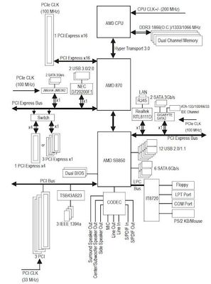
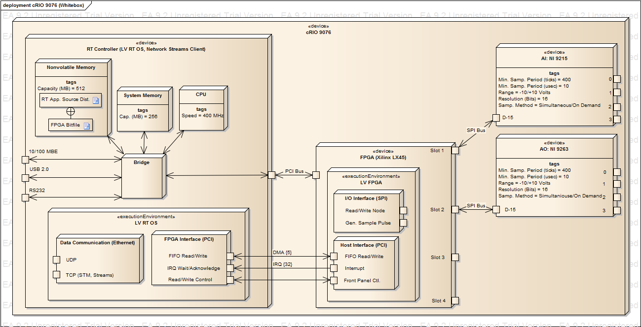
I'm trying to work up a document on our cRIO 9076 for the lab, and I'd like to include a schematic/block diagram of its overall internal structure...something like what PC motherboard makers give (example below). The internals of the RT controller are pretty easy to guess at, but I'm a little fuzzy on the connections between that and the FPGA, and between the FPGA and the chassis modules. Any pointers on where I should be looking (not in the manual, by the way)?
Thanks a bunch.
02-22-2012 11:09 AM
- Mark as New
- Bookmark
- Subscribe
- Mute
- Subscribe to RSS Feed
- Permalink
- Report to a Moderator
Hello bcro,
I haven't seen any internal block diagrams for the cRIO similiar to the one that you've posted. The closest I could find is the first figure seen in this article. There are block diagrams for our R-series cards however. You can find them in the manual here starting at page 2-1. They won't be exactly the same but leads to and from the FPGA will be similiar.
David A
02-27-2012 07:10 PM
- Mark as New
- Bookmark
- Subscribe
- Mute
- Subscribe to RSS Feed
- Permalink
- Report to a Moderator
David--
Thanks a bunch for your reply. That manual got me pointed in the right direction. I also found this little wiki stub:
http://en.wikipedia.org/wiki/CompactRIO
which specifies the controller-fpga connection as PCI, meaning much of the details are probably obvious with a better understanding of PCI busses. In any case, I've managed to start a diagram of my own that will suit my needs just fine.
Thanks again, and have a great day.


