- Subscribe to RSS Feed
- Mark Topic as New
- Mark Topic as Read
- Float this Topic for Current User
- Bookmark
- Subscribe
- Mute
- Printer Friendly Page
Here are 40000 points (x,y) on the wafer, how to arrange them into the right row/column, in order to form wafer map?
12-28-2013 01:11 AM - edited 12-28-2013 01:33 AM
- Mark as New
- Bookmark
- Subscribe
- Mute
- Subscribe to RSS Feed
- Permalink
- Report to a Moderator
Hello all friends,
I want to arrange all these phisical points into a logical map, but how many rows and column are not known in advance, we just know:
1. seperation can be given, for example stepX(width) =390.7,StepY(heigh) =318.8
2. some of the points' posX and posY are scaned several times, so deleting redundant data needed.
What's the method to solve this problem?
posX posY
60346 79682.2
59928.4 78089.2
60724 79044.4
61484.2 78085.9
59948.7 79045.6
61479 77767.5
60339.5 79365.1
56052.5 79061.7
56030.9 78113.6
56428.6 78425.4
56436.5 78745.9
57201.8 78106.2
58781.1 79374.2
56448.4 79702.1
56825.3 79066
56440.2 79059.4
57613.9 79700.8
56840.8 79699.7
57989.3 78739.6
58778.9 79692
58772 79048.6
58004.9 79692.7
56057.1 79703.9
57224.6 79381.9
56821.8 78747.1
56422.6 78111.7
57611.8 79379.9
56047.5 78747.2
56827.9 79385.8
56416.1 77793.6
57194.1 77787.8
56048.2 79385.7
58383.6 79060.5
56444.7 79384.2
57587.1 78109.3
......
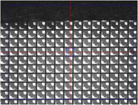
Below is a small example to demostrate this case, just with hundreds of points
From sacnning the wafer:
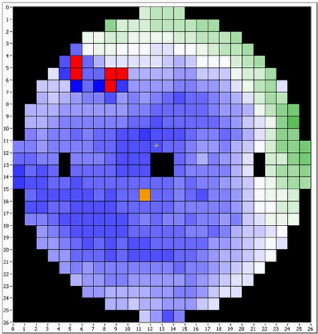
To form the map:
Thanks very much,
Deho
12-28-2013 08:01 AM
- Mark as New
- Bookmark
- Subscribe
- Mute
- Subscribe to RSS Feed
- Permalink
- Report to a Moderator
Deho,
The intensity graph can produce displays like your wafer map image. The intensity graph uses the indexes of the input 2D array as the values for the axes, although the origin is at lower left rather than upper left as in your image. That can be handled by reversing the order of the rows in the array. Because the axes are integer-based, you cannot easily get a display with different stepX and stepY. It could be done by duplicating points, but the arrays would get very large and the display prbably would not have enough pixels to resolve everything anyway. Your image appears to use squares in the map so this may not be an issue.
Since your position values are not integers, finding the dupilcated positions may be difficult. You cannot just use equality comparisons on floating point numbers and expect good results. A value like 390.7 (the stepX value in your example) cannot be represented exactly in binary. So if you get the various posX values by repeatedly adding stepX to the previous posX, you may not always get exactly the same binary number when you come back to a particular value. The comparisons would need to be (posX[j] - delta <= posX[i] <= posX[j] = delta) where delta is a value you choose to be larger than the round off error and less than the step size.
Another consideration: When a point is measured multiple times, the result will not always be identical due to noise and measurement imperfections. How do you choose which of the duplicated valeus to use? Taking an average of all the duplicates at a point might be one way to reduce the effects of noise, but will require more effort to write the code.
You would also need to sort the values so that the indexes (axis values) correspond to increasing values of posX and posY.
Lynn
12-29-2013 03:51 AM
- Mark as New
- Bookmark
- Subscribe
- Mute
- Subscribe to RSS Feed
- Permalink
- Report to a Moderator
Hi Deho,
What is the die size (x & Y) for your data set?
If you arbitrarily set the row and column of the first XY pair to 0,0, you could calculate the relative row and column of the next XY pair as:
(X Pos(0) - X Pos(1)) / Die X size = Relative Column for XY pair(1)
(Y Pos(0) - Y Pos(1)) / Die Y size = Relative Row for XY pair(1)
Loop through your data to create a Row/Column array.
The accuracy of your scanned XY position values must be tested to see if you need to add some
additional manipulation of the data along the line of what Lynn suggested.
steve
Help the forum when you get help. Click the "Solution?" icon on the reply that answers your
question. Give "Kudos" to replies that help.
--------------------------------------------------------------------------------------------------------------------------
12-29-2013 04:27 AM - edited 12-29-2013 04:28 AM
- Mark as New
- Bookmark
- Subscribe
- Mute
- Subscribe to RSS Feed
- Permalink
- Report to a Moderator
Hi Deho,
please give a link and some remarks when using other people's work in your posts - like you did by using a picture posted by me from a wafer mapping tool I wrote once! Atleast you informed me with a private message...
- You should work with chip numbers (you surely use them?) instead of arbitrary XY positions of a wafer probing tool. If that is not possible you should calculate the chip number from the given XY data.
- It's no problem to not knowing the actual wafer size before reading the data, you can scan the data for min/max positions to calculate wafer (and array) size...
- Once you know the number of chips you can initialize a 2D array with an element for each chip and copy the measured values into that array. Then just display that array in an intensity graph.
- You might need to change the default Z axis (color ramp) of the graph to fit your needs...
12-29-2013 05:42 AM
- Mark as New
- Bookmark
- Subscribe
- Mute
- Subscribe to RSS Feed
- Permalink
- Report to a Moderator
Thanks Johnsol,Stevem181 ,GerdW:
display using intensity chart with 2D array data source can be realized, there are some topics discussing about it. For example, from Stevem181(thread here), and GerdW (thread here).
And, thanks GerdW again, I use the map image from his post, everybody can goto that thread for detailed. .
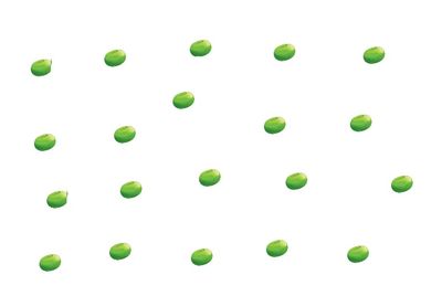
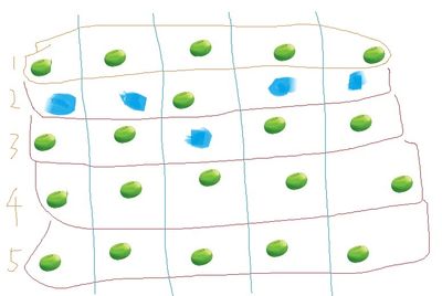
but, I think the diffcult may be the classfication of the data. The question is like this, let me give an example: Throwing a handfull of beans on the desktop, under this condition without anyother infomation supported, how to segment them in to the best suitable row/coulmn?
for example this is the case:
here is classfication 1:
and here is the classfication 2:
In these two arrangement surely we think 1th is more suitable than 2th,
for there are too many empty cells in 2th , indicated by blue color::
12-29-2013 10:27 AM
- Mark as New
- Bookmark
- Subscribe
- Mute
- Subscribe to RSS Feed
- Permalink
- Report to a Moderator
Hi deho,
I can live with your 2nd classification too. No problem with empty cells...
- I said "graph", not "chart". It's quite a difference!
- In your first post you claimed, that there is a known stepwidth for X and Y each. So why do you work with random positions now?
- You can create histograms of X and Y positions. Use them to decide on the number of rows/columns. The more coarse you select them, the more chips will be handled by one wafer mapping position. The finer you separate the XY positions the more empty cells will remains. It's your decision...
12-29-2013 07:29 PM
- Mark as New
- Bookmark
- Subscribe
- Mute
- Subscribe to RSS Feed
- Permalink
- Report to a Moderator
Thabks GerdW,
Yes, the stepX/Y was know , and in fact this parameter can be calculated from the data set, rather than from users input, but this parameter could not be used strictly.
There are 2 factors about this question, the fist is noise in measurement, the other is more difficult, int the large disc, there will be a slope in the edge, like this:
so, I think, maybe we should just deal with the dataset, the other information, such as stepX/Y, die size, disc diameter, can only be treated as reference, I do't know is it true
12-29-2013 07:42 PM
- Mark as New
- Bookmark
- Subscribe
- Mute
- Subscribe to RSS Feed
- Permalink
- Report to a Moderator
I have an idea, but not a algorithm:
1. firstly, arbitrarily select one point as the starting seed point;
2. then, arbitrarily define deltaX/deltaY as the criteria, from the starting seed point , searching its neighbor around, in up/down/lef/right all directions.
Then arrange them into the same line, or increase the row, or decrease the row, according the delta value, iteration...
When the last point in the data set was reached, then get one sollution, a map;
3. then, repeatly tuning the deltaX/deltaY value, will get may many solutions, that say, many maps;
4. finally, among these solutions under different deltaX/deltaY, estimate the best solution, accoarding to some criteria, for example, if the empty cells minimal? or if the row+column minimal, or if the connection region max? then we set this solution as the map we needed.
maybe the processing time is unimaginable...
09-29-2017 04:23 PM
- Mark as New
- Bookmark
- Subscribe
- Mute
- Subscribe to RSS Feed
- Permalink
- Report to a Moderator
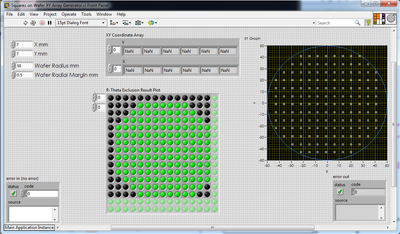
Not exactly on topic, but here is a VI that will 'draw' a grid within the boundaries of a circle (squares on a wafer). This is basic to wafer/motion navigation.
I am posting this, as I cannot find any example Vi's sans a $$ toolkit.
Regards, use openly and freely!
Jack Hamilton
