- Subscribe to RSS Feed
- Mark Topic as New
- Mark Topic as Read
- Float this Topic for Current User
- Bookmark
- Subscribe
- Mute
- Printer Friendly Page
Disappointed annoyed and angry:: merge labview fpga with vhdl through ip block
12-17-2013 02:31 PM
- Mark as New
- Bookmark
- Subscribe
- Mute
- Subscribe to RSS Feed
- Permalink
- Report to a Moderator
dear member
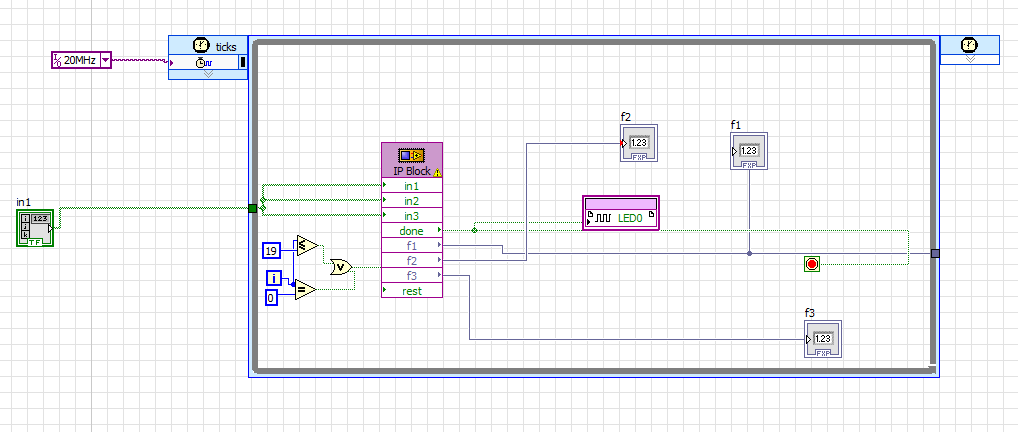
after i complete vhdl developing i successful merge the vhdl code with labview fpga like in figure below
when i make a simulation for this figure the system work well and give right result
but when i test in hardware the result is wrong ??? why why !!!! what can casue that
help member help
12-17-2013 02:36 PM
- Mark as New
- Bookmark
- Subscribe
- Mute
- Subscribe to RSS Feed
- Permalink
- Report to a Moderator
In what way is the result wrong (does not work, off by a few %, something else?)
12-17-2013 02:38 PM
- Mark as New
- Bookmark
- Subscribe
- Mute
- Subscribe to RSS Feed
- Permalink
- Report to a Moderator
@altenbach wrote:
In what way is the result wrong (does not work, off by a few %, something else?)
dear the result is wrong 100%
for example the result must be 3.99..
in hardware i get -0.00349..
12-17-2013 02:40 PM
- Mark as New
- Bookmark
- Subscribe
- Mute
- Subscribe to RSS Feed
- Permalink
- Report to a Moderator
Can you post this code so the community can take a look?
12-17-2013 02:44 PM
- Mark as New
- Bookmark
- Subscribe
- Mute
- Subscribe to RSS Feed
- Permalink
- Report to a Moderator
@Dragis wrote:
Can you post this code so the community can take a look?
it about 800 row vhdl
i will but them complete soon with labview fpga project so its easy for member to test
12-18-2013 12:49 AM
- Mark as New
- Bookmark
- Subscribe
- Mute
- Subscribe to RSS Feed
- Permalink
- Report to a Moderator
Well, did you notice the warning triangle in the logo of the IP Integration Node? That is the sign of possibly not having consistent result between your simulation and your hardware running. This is because your vhdl doesn't have any clock enable signal and thus your IP Integration Node starts to run before the other nodes on the diagram "wake up" (The other nodes are freezed by the clock enable.)
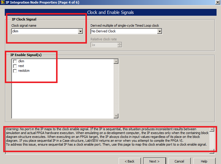
This warning of possible different behavior is shown on the page of enable signal selection of the IP Integration Node wizard. You can jump in there and have a close look.
12-18-2013 06:44 AM - edited 12-18-2013 06:46 AM
- Mark as New
- Bookmark
- Subscribe
- Mute
- Subscribe to RSS Feed
- Permalink
- Report to a Moderator
@david1147 wrote:
Well, did you notice the warning triangle in the logo of the IP Integration Node? That is the sign of possibly not having consistent result between your simulation and your hardware running. This is because your vhdl doesn't have any clock enable signal and thus your IP Integration Node starts to run before the other nodes on the diagram "wake up" (The other nodes are freezed by the clock enable.)
This warning of possible different behavior is shown on the page of enable signal selection of the IP Integration Node wizard. You can jump in there and have a close look.
Dear
thank for your note
the problem is I didn't find any white paper from NI for how to make a right merge between labview fpga and VHDL
I always note this warning triangle in the logo of the IP Integration Node but I didn't know what is best vhdl programming method to make this warning triangle disappear
for example the vhdl process configuration for counter is :
process(clk,rest)
begin
if(rest='1') then
coun:=0;
elsif( rising_edge(clk) ) then
coun:=coun+1;
end if;
end process;
-----------------------
so during IP block configuration for my system we can see the warring appear as shown in figure below
so dear what is mean by clock enable signal??? Can your modified the vhdl code for counter code to have clock enable???
Best regards
12-18-2013 08:25 AM - edited 12-18-2013 08:27 AM
- Mark as New
- Bookmark
- Subscribe
- Mute
- Subscribe to RSS Feed
- Permalink
- Report to a Moderator
For this specific case, you can modify your code to be something like this:
process(clk,rest)
begin
if(rest='1') then
coun:=0;
elsif( rising_edge(clk) ) then
if cClockEnable='1' then
coun:=coun+1;
end if;
end if;
end process;
12-18-2013 12:45 PM - edited 12-18-2013 12:46 PM
- Mark as New
- Bookmark
- Subscribe
- Mute
- Subscribe to RSS Feed
- Permalink
- Report to a Moderator
Great catch @david1147, I didn't see that tiny triangle originally. Yep, when you see those warning symbols that is definitely the place to start looking. And as a good development practice, if a warning triangle is intentional and necessary it is good to put a comment on the diagram explaining why it is necessary so when you or someone else comes back to it in the future you don't have to figure it out again.
12-21-2013 07:40 AM - edited 12-21-2013 07:44 AM
- Mark as New
- Bookmark
- Subscribe
- Mute
- Subscribe to RSS Feed
- Permalink
- Report to a Moderator
Dear members
I I apologize for not answering for a period as I Decided to divide the system into parts and make a hardware debug to know the place of wrong and this Simplify My problem and can be tested
my problem now is in unit that is responsible for take absolute value for negative numbers and keep positive number with out any change
the labview FPGA with ip block simulation give me right result
but in hardware test the result when i put positive number is wrong (the positive number is converted to negative number)
for example
when i put -1==>1 ok
but when i put 1 ===>-1 this wrong
from below code this case in labview fpga simulation this case will executed right
case es is
when "0100" => t1:=suma2; ----positive number
when "1000" => temp0:=not(suma2); --- negative number so take abs (not+1)
t1:=resize(temp0+onf,t1);
WHEN OTHERS => null;
end case;
but in hardware this part of code of case structure will always executed and this causes an wrong result for positive numbers
when "1000" => temp0:=not(suma2);
t1:=resize(temp0+onf,t1);
any help ??? Any change for case !!!
Complete code for process
process (clk) variable temp0,t1:sfixed(3 downto -12); begin if (rising_edge(clk)) then if(ec='1') then es2<=es; ------------------------------take abs value------------ case es is when "0100" => t1:=suma2; when "1000" => temp0:=not(suma2); t1:=resize(temp0+onf,t1); WHEN OTHERS => null; end case; out11<=to_slv(t1); end if; end if; end process;


