From Friday, April 19th (11:00 PM CDT) through Saturday, April 20th (2:00 PM CDT), 2024, ni.com will undergo system upgrades that may result in temporary service interruption.

We appreciate your patience as we improve our online experience.

LabVIEW FPGA Idea Exchange

Community Browser
cancel
Showing results for 
Search instead for 
Did you mean: 
Post an idea

When dragging multiple IO items from project to a block diagram, it'd be great to have them show up as a single IO node instead of multiple ones. To be backward compatible it could be something like <Shift>-drag. This improves code readibility by producing more compact code.


AndreasStark_0-1680632105226.png


Hello,


I recently have issue configuring FPGA Vis to be run seemlessy by the same host code, because of incompatible interface between VIs. Here is the Configure FPGA VI Reference Interface :


Configure FPGA VI Reference InterfaceConfigure FPGA VI Reference Interface


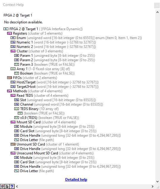
And here are two (differents) interface, fore FPGA 1.vi and FPGA 2.vi respectively, as seen in the context help. I just duplicate the VI for the example and get the tab order modified - see under Registers :


Context Help for FPVA 1.viContext Help for FPVA 1.viContext Help for FPVA 2.viContext Help for FPVA 2.vi


I think it could be more consistent to have the same kind of display in the configure dialog, with the same control order. It's quite confusing not seeing any difference when configuring a reference to discover that something is wrong at run-time (controls and indicators are separated, and then sorted alphabetically - I only set controls in my example code, no indicators). The context help over the dynamic reference finally helps me to figure out what was wrong but it tokk me a while...


Please note that the FPGA FIFOs have to be define if the same order from one bitfile to an other (if there is differents targets, or differents projects). This is correctly reflected by the configuration window.


So I suggest having a more coherent display of control and indicators interfaces, that correspond to the effective interface (just like the context help does), i.e. the tab order of the controls under Registers.


Best regards,

As somewhat an opposite request to this idea

https://forums.ni.com/t5/LabVIEW-FPGA-Idea-Exchange/Ability-to-define-datatype-of-Registers-FIFOs-from-code-without/idi-p/3123936

I would like to show some pertinent information to the configuration of certain primitives in FPGA code.


Intaris_0-1663335955202.png


The ability to turn this display on and off just like a label would be very welcome indeed. I'd always have it visible.


I just spent two days tracking down a bug which ended up being an under-dimensioned Block RAM instantiation (and how BRAM indexing works, just throwing bits away instead of coercing the read/write index), something whose configuration is completely hidden from view. Why can't we have some visible elements to show the size of a Block RAM and the Datatype (FXP would do for any given FXP type). Same goes for FIFOs, whether a FIFO is 16 elements or 8192 elements deep is a very important piece of information. And of course I mean only the primitives which instantiate the resources, not FP references for these items, even though the datatype of these would also be a very welcome addition.

With even simple examples we experience errors when trying to run Instruction Framework based LabVIEW FPGA VIs.


This is a blocker for our using Instruction Framework.

MGT interfacing to the 7915 is provided: https://forums.ni.com/t5/Examples-and-IP-for-Software/Aurora-64b-66b-Streaming-Example-for-the-PXIe-7915-Ultrascale/ta-p/3952187


It is not provided for other cards such as the 5785.  Is the interfacing the same?  Could examples for this be provided?

Working with the NI 5785 our team had a hard time understanding how to use TClk without all of the extra (e.g. streaming) code that comes with the example.


Through support we were eventually put in touch with R&D and they told us how to initiate TClk by setting some of the FPGA controls.  This was helpful but not intuitive.


TClk helps support beamforming applications shown in the NI Marketing but without this usability it is very difficult (impossible) to develop applications promised.


TClk also has other lower level features such as the delay correction.  No info is posted on this either but it is a property we can read.

When not using Instruction Framework to interface from the Host to LabVIEW FPGA the FPGA VI reference register items cannot be ordered by the user


They appear in a random order (order of creation) and it is not easy to find and select them.


I am referring to this function: https://zone.ni.com/reference/en-XX/help/371599P-01/lvfpgahost/readwrite_control/

The rvi folder has automation tools for FPGA compiles.  These are not very well documented.  There are no examples on using these.


Could additional info and examples be provided?


This is useful for projects where automated building helps continuous integration with tools such as Jenkins or Bamboo.

One of the benefits of the Instruction Framework is that one could develop several modules each using Instruction Framework.  The modules can then be integrated and the Instruction Framework modules can be assembled using Collections.


This information is not clear and the provided tutorial does not provide information on this use case.

LabVIEW NXG had the ability to create a resource file.  Though I cannot find the help reference for this I will describe the functionality below:


Right now the Target Scoped FIFO, P2P, DMA-FIFO, Memory, Handshake Items, Registers, Clocks, etc are all stored as part of LabVIEW Project (lvproj) file.


If want to port to a new project file or target I have to copy/paste.  This is not a big deal and works well.  However if I update one project's configuration I have to re-copy/paste.  From a configuration management perspective I cannot ensure the configurations are always the same.  With larger, multi-FPGA projects this becomes critical.


It would be great to have a file that holds all of these resources to allow for easier portability and configuration management.

When we try to compile timing critical FPGA application, if might be failed because of timing violation.

But if it missed only a few nanoseconds, recompiling might resolve the error as below.


Resolving Timing Violations on the FPGA

If your failed compilation misses the required throughput time by only a few nanoseconds, try rebuilding your bitfile. Each build of a bitfile does not always produce identical results on the FPGA, so rebuilding sometimes resolves minor timing violations. 


In most case, compilation might require much time and it's difficult to take quick action after they found the aborted compilation result.

It would be great there is an option which allow automated recompile like below.

Of course the compilation completed, it wouldn't try recompile. Only failed, try to compile again.


** -------------------------------------------------------------------- **

Enable Auto Recompile [  *  ]   Number of Retry  [  4  ]

** -------------------------------------------------------------------- **

Default interface for FIFOs is Timeout (https://zone.ni.com/reference/en-XX/help/371599P-01/lvfpgaconcepts/fpga_interface_options/)


I would prefer the default be Handshaking.

The 7976 and 7915 have certain functions (e.g. Basic Elements) in different locations.  Some do not even show up (e.g. Channel is in 7976).


NI 7976 LabVIEW FPGA 2018:


Terry_ALE_0-1600126303727.png


NI 7915 LabVIEW FPGA 2018:

Terry_ALE_1-1600126401252.png


Hello,


Is there any possibility to use a dedicated file to change the Number of Synchronizing Register


Today we need to right click on the DIO + Propriety + Advanced Code Generation + Select Nb of register.

On a SBRIO 9607 I have to do it 96 times and if I change something with the CLIP generator I need to do it again.  

In my design I use VHDL IP so the synchonisation is already done on the VHDL and I don't need extra clock.

2020-01-24_07h57_17.png


I try to edit with Notepad++ the .lvproj file and change the NumberOfSyncRegistersForReadInProject or NumberOfSyncRegistersForOutputData but it's not clean...


If you have an idea it will save a lot of click.

Thanks

Perhaps there's already a good way to do this, but some structures/nodes are allowed in a Single-Cycle Timed Loop but their behaviour is significantly changed, perhaps breaking your VI.

It would be good to be able to mark VIs in some way as unsuitable for use within a SCTL.


An example is the flat sequence structure - you can place this in a SCTL and it can pass intermediate file generation, but the behaviour is as if there was no sequence structure.

Assuming that it isn't always superfluous, this probably indicates invalid behaviour but is not necessarily obvious to detect (e.g. with broken compilation or intermediate files).


Some specific node that could be placed on a block diagram and indicate that a VI cannot be placed inside a SCTL would be useful.

Something like a Divide can be used for this, but not trivially easily - you need to actually use the output of the Divide or else the dead-code elimination allows the intermediate files to be happily generated. It took me quite a few goes to get a failure even with SGL precision divide in a SCTL... wiring to a structure or an indicator is not enough, it must be something that actually uses the value.

Initially I looked around for my previous idea here: Selecting between two I/O refnums not allowed because I thought it was the same and intended to post a comment to that, but I see that was a bit more specific.


This seems like a more allowable case - why is A forbidden and B perfectly ok?


A:

Select node in SCTLSelect node in SCTL


B:

Case Structure to choose between two values based on boolean inputCase Structure to choose between two values based on boolean input


Here A is forbidden (at Intermediate file generation - so perhaps this would help: Unsupported nodes inside for loop within SCTL should result in a broken VI (NXG != Already Implemented really...)) but B is compiled with no problem. I really don't see why Select of two integers is different to a Case Structure with two integers input, a boolean case selector, and an integer output from the two inputs...


As an idea rather than a rant, I'd like A to be possible.

Better visual indication of estimated and final timings in compilation report.


Would it be possible to add some visual clues as to whether a given clock in an FPGA design has been met or not? Maybe a background colour, green for good and red for bad?


color clocks.png

Sometimes it's really hard working out which clocks have met timing and which not.

It would be nice if this code:

Case Structure versionCase Structure version


could be replaced by this code:

Select versionSelect version


but doing so gives an edit-time error specifying that "Select: Possiblity of Dynamic Refnum not supported for current target".


Is there a fundamental reason this can't be allowed? The behaviour is presumably the same in each case, and the references are from the same place in both cases. In the case structure, the exact same references that are passed to the Select node are used, with the same True/False choice.


It's not a huge issue, but it would be a nice usability/readability improvement.

Arising from similar requirements as I have posted many moons ago: HERE.... I naively thought putting a terminal in a disable structure would remove it from the FPGA compile. It doesn't.


Years later, I have developed a nice debug interface for my FPGA code which is becoming more and more modular as I refactor it.  I have many sub-modules with their own debug interfaces which can be turned on or off from the top-level VI via LVOOP method injection.


The problem is that I can't really compile my entire FPGA VI with ALL debug paths enabled as this just won't fit (It will sometimes compile, but most often not and our FPGA code base is still growing).  And this is before I even think about making my debug information more detailed.  I would like to be able to easily switch certain aspects of the debug interface on and off as testing requirements change.  On the debug interface level I can do this easily by simply not reading the data from the objects being used for the data transfer or simply passing in abstract methods which don't actually do anything and get optimised away.  But I'm left with a load of FP controls which are still eating up resources on the FPGA target. Smiley Mad I don't want to delete the controls because that leads me to X copies of ever-so-slightly out-of-sync versions of my test VI which quickly becomes a maintenance nightmare.  Instead, I want to be able to "easily" reconfigure my test front-panel to only compile the stuff I'm currently actually interested in.


Part of what I would like is the ability to actually define areas of the FP which are enabled, disabled or enabled (and preferably also based on whether simulation is active or not - hence conditional disables for FP).  This way, when compiling, the FP elements will actually disappear and full resource savings can be made (as Xilinx is clever enough to optimise away any pointless code LV may stillhave instantiated in VHDL).  In addition, the ability to define certain controls as being enabled only when in simulation mode can allow us to have SGL graphs and so on present when needed during debugging.


So, would having conditional disable options for the FP (where controls are shown as greyed out when not available) be of interest to anyone?  If this would be an FPGA only thing, I wouldn't shed and tears.


Am I the only one who would use this? hmm. Maybe.

Please add the ability to right-click on a Memory, Register and/or FIFO and FIND ALL instances throughout the project and/or VI hierarchy. Ideally it would be just like local and global variables (as shown) for desktop LabVIEW. 


FIND all instances for BRAMs.png