- Subscribe to RSS Feed
- Mark Topic as New
- Mark Topic as Read
- Float this Topic for Current User
- Bookmark
- Subscribe
- Mute
- Printer Friendly Page
Can we decoding Double Data Rate data at SBRIO?
12-12-2015 04:04 AM
- Mark as New
- Bookmark
- Subscribe
- Mute
- Subscribe to RSS Feed
- Permalink
- Report to a Moderator
Dear All:
I learned quite a lot from this community, and I'd like to thanks you all for your time.
There is one thing I did figure out yet, can we decoding DDR data?
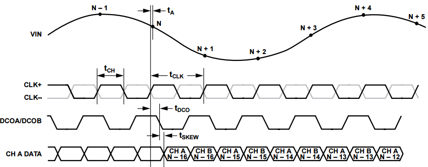
The picture below is a timing diagram of a highspeed ADC, the CLK+/- is ADC clock input, and the DCOA/B can be used as ADC clock out according to datasheet.
Say that I put my sbrio to use external clock which is DCOA in the diagram, and let's assurme the clock runs at 120MHz, I can make my SCTL running at the same speed that driven by DCOA, but only will be able to readout one channel's data.
Optional solution 1:
Put a NOT gate at DCOA, and put another SCTL base on a negtive clock, it might function.
But it also might introduce some degree of delay, which might make the system less stable.
Optional solution 2:
Set a derived clock at 2 times of the orginal ADC clock, and sample odd and even clock and put them at different FIFO or so.
The speed would be very much out of control, 120M SCTL works fine with me, I'm prety sure that will work, but 240M SCTL are kind too much for 9651, even a little change in code might make it fail to compilation, also it seem would lead to more power consumption, which is not perferable in my application.
Optional solution 3:
What if I can change the SCTL's phase of the input clock, say that I could configure one SCTL to running at 0 degree, and set another SCTL running at 180 degree, everything will works like it spossed to be, no extra external component needed, no 240M coding needed.
-----------------------------------------------------------------------------------------------------------------------------------------------------------------------------------
So the question would be, can I confurige the from CLIP clock somehow, to make it locked at differernt phase of inputted clock? I don't need it to be too flexible, only positive or negtive the clock would be fine with me.
Or we can look it from another aspect, if the default SCTL triggered at the falling edge of external clock, can I configure another clock that triggered at the rising edge?
Thanks!
12-13-2015 11:22 PM
- Mark as New
- Bookmark
- Subscribe
- Mute
- Subscribe to RSS Feed
- Permalink
- Report to a Moderator
Hi JiangLiang,
The best way to recieve a DDR signal is to use the IDDR primitive within the FPGA. These blocks are in the input/output block of the FPGA and will deserialize the incoming DDR signal to two SDR signals. You can then read the two SDR signals using a normal SCTL in labview. Doing this requires manually editting the CLIP's VHDL file. Below is a simple example of how to do this, and the example's CLIP.
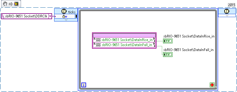
1. In the clip generator create a boolean read-only LabVIEW port named DataInRise, assign this to the DIO connected to the DDR data. Create another boolean read-only port namded DataInFall. Do not assign this port to a DIO.

2. Create your incoming clock as normal.
3. Go to the CLIP output directory and open the CLIP's vhd file in a text editor. Scroll down till you see the following:
--------------------------------------------------------------
--LabVIEW Port: DataInRise
---------------------------------------------------------------
DataInRise_lv_in(0) <= aDio_in(0);
---------------------------------------------------------------
--LabVIEW Port: DataInFall
---------------------------------------------------------------
DataInFall_lv_in(0) <= '0';
---------------------------------------------------------------
--LabVIEW Clock Port: DDRClk
---------------------------------------------------------------
DDRClk_lvc <= aDio_in(15);
4. Replace this section with an IDDR instantiation. It should look like this:
-- IDDR: Double Data Rate Input Register with Set, Reset
-- and Clock Enable.
IDDR_inst : IDDR
generic map (
DDR_CLK_EDGE => "OPPOSITE_EDGE", -- "OPPOSITE_EDGE", "SAME_EDGE" or "SAME_EDGE_PIPELINED"
INIT_Q1 => '0', -- Initial value of Q1: '0' or '1'
INIT_Q2 => '0', -- Initial value of Q2: '0' or '1'
SRTYPE => "ASYNC") -- Set/Reset type: "SYNC" or "ASYNC"
port map (
Q1 => DataInRise_lv_in(0), -- 1-bit output for positive edge of clock
Q2 => DataInFall_lv_in(0), -- 1-bit output for negative edge of clock
C => aDio_in(15), -- 1-bit clock input
CE => '1', -- 1-bit clock enable input
D => aDio_in(0), -- 1-bit DDR data input
R => aReset, -- 1-bit reset
S => '0'
);
---------------------------------------------------------------
--LabVIEW Clock Port: DDRClk
---------------------------------------------------------------
DDRClk_lvc <= aDio_in(15);
5. In your SCTL running on DDRClk, read both DataInRise and DataInFall each cycle. The SCTL will only execute on the rising edge of DDRClk. Reading both DataIn signals will give you your DDR data.
For more information on the IDDR primitive see the Xilinx Select IO User Guide at:
http://www.xilinx.com/support/documentation/user_guides/ug471_7Series_SelectIO.pdf
For example Xilinx primitives instantiations in VHDL see the HDL Library Guide at:
http://www.xilinx.com/support/documentation/sw_manuals/xilinx14_7/7series_hdl.pdf
NI Chief Hardware Engineer
08-03-2019 02:34 PM
- Mark as New
- Bookmark
- Subscribe
- Mute
- Subscribe to RSS Feed
- Permalink
- Report to a Moderator
Hello Nathan,
I used your way to successfully receive one DDR output data from ADC. But ADC have mutiple channels, when I instantiate IDDR for more than one channels, there will be error report. How can I use IDDR for multiple channels?
08-05-2019 10:57 AM
- Mark as New
- Bookmark
- Subscribe
- Mute
- Subscribe to RSS Feed
- Permalink
- Report to a Moderator
What error are you encountering? Could you attach screenshots of the error code/text as well as the portion of the CLIP where you instantiated your IDDR components?
Thanks,
Will
National Instruments
08-05-2019 04:21 PM
- Mark as New
- Bookmark
- Subscribe
- Mute
- Subscribe to RSS Feed
- Permalink
- Report to a Moderator
Hello Wilbur,
I'v solved the problem. I used the same IDDR instantiation name for multiple output. It's a stupid mistake.
Thanks for your reply.
