From Friday, April 19th (11:00 PM CDT) through Saturday, April 20th (2:00 PM CDT), 2024, ni.com will undergo system upgrades that may result in temporary service interruption.
We appreciate your patience as we improve our online experience.
From Friday, April 19th (11:00 PM CDT) through Saturday, April 20th (2:00 PM CDT), 2024, ni.com will undergo system upgrades that may result in temporary service interruption.
We appreciate your patience as we improve our online experience.
04-03-2015 04:07 AM
Hi all,
I plan to use the sbRIO9651 SOM with our own PCB. The sbRIO will sit on the top of our PCB and the two systems will communicate via the Mezannine connector. I have to use LVDS signals (both inputs and outputs).
Can I use LVDS (in and out) from those banks which is powered from 3.3V? What will be the common mode voltage for the LVDS out signals (powered from 3.3V VCCO pins)?
Thank you.
04-03-2015 07:04 AM
Table 12 in the sbRIO-9651 user manual lists the IO standards and appropriate nominal supply voltages. The LVDS standards in the table require 2.5V.
Table 15 specifies the common mode input and output voltages for LVDS pairs - min, max, and typical.
http://www.ni.com/pdf/manuals/376962b.pdf
The sbRIO CLIP generator (used to configure the capabilities of all IO on the SOM) has rule checking in place to ensure your IO configuration is valid before generating a CLIP.
Spex
04-03-2015 08:41 AM
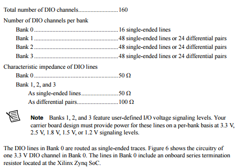
You'll also be interested in the specifications/text just above Table 12 (top of page 16). To answer your initial question in short though, the Bank 0 DIO (DIO 0-15) can only be used as Single-Ended 3.3V.
As for the rule checking part that Spex mentioned, this is what will happen if you try to choose LVDS for Bank 0.
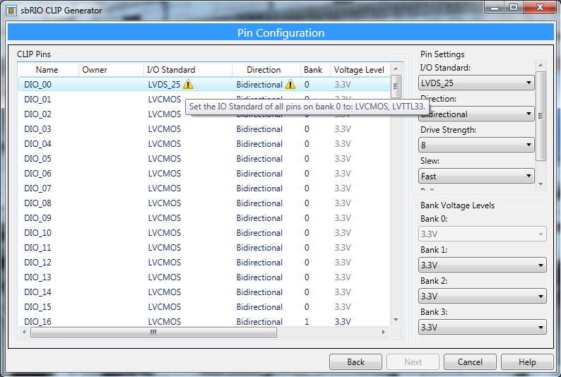
In general, as you're developing your pinout, I would recommend testing that pinout with the sbRIO CLIP Generator. Because we have rule checking in place, it will help make sure you are properly using the I/O from the board and help catch any issues before investing time in layout/fab/testing. Also, as an added benefit, you'll already have your socketed CLIP developed for the LabVIEW project.
Eric
04-06-2015 07:38 AM
Dear Gentlemen,
Thank you for your quick responses.
If I use 2.5V VCCO for a bank (where LVDS pairs are located) and I define LVCMOS_25 pins (single ended) then can these LVCMOS_25 pins tolerate 3.3V (our LVCMOS_25 pins are input and they are driven by external 3.3V CMOS outputs)? Should I add serial resistors (about 1K) to limit the current?
Thank you again for your help,
Gabor
04-06-2015 12:25 PM
Hi Gabor,
If you need to route a 3.3 V single-ended signal to the same bank that is also routing a 2.5 V LVDS signal, I would recommend buffering the 3.3 V signal to 2.5 V and configuring the sbRIO CLIP Generator as LVCMOS_25.
Of course, I only recommend this if it is a requirement that you use the same bank to route LVDS and 3.3 V CMOS. If your application allows, the better option is to use one of the 16 DIO signals that are already 3.3 V, single-ended (DIO_0 through DIO_15). All lines on Bank 0 are powered by VCC_3V3.
Alternatively, if Bank 0 does not work for your application, you can power different bank that is not routing differnetial DIO and power that at 3.3 V. Regardless of if you use all of the banks, you are still required to supply a bank voltage. Since VCC_3V3 is easily accessible already, you can use same supply to power the unused banks.
- Tanner
04-27-2015 10:16 AM
Dear Gentlemen,
thank you again for your help. It seems I can configure the sbRIO CLIP Generator as I'd like to but I cannot find wherre and how to set 100 ohm differential termination on LVDS input pin pairs. Do you have any idea?
Regards
Gabor
04-27-2015 12:52 PM
Hi Gabor,
When you configure a DIO pair as LVDS inputs, the CLIP generator automatically enables the 100 Ohm internal differential input termination on the pair. You can verify this by inspecting the contraints file (.xdc) generated by the CLIP generator in the same folder as your CLIP .vhd, .xml (for LabVIEW), and .cfg (Config settings for the Generator). For example, here is the entry in an .xdc file for a differential input I created in the CLIP generator.
#################################################################
# DIO_16
#################################################################
set_property IOSTANDARD LVDS_25 [get_ports {aDio[16]}]
set_property DIFF_TERM TRUE [get_ports {aDio[16]}]
The last page of the CLIP generator will include a path to where these files are placed on disk.
Regards,
spex
05-14-2016 11:18 PM
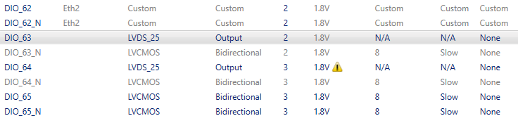
I noticed a very funny issue about LVDS, when I enable ETH2, the CLIP Generator force me to set bank 2 to 1.8V, but at the same time, I can use LVDS at bank 2? But I cann't set Bank 3 with 1.8V voltage with LVDS without Warinig Mark.
Is there some thing going on underneath, or is this just a software error?
I would like to have my ADC running at logical IF with 1.8V, yet to have a better clock performance, I would like to provide my clock with LVDS, in the same bank would make things less messy.
05-16-2016 10:23 AM
This looks like a software error. I just tried it out and the bitfile compilation fails with
ERROR: [DRC 23-20] Rule violation (BIVC-1) Bank IO standard Vcc - Conflicting Vcc voltages in bank 33
There should be a warning glyph for this.
05-20-2016 10:35 AM
Hi Jiangliang,
The Zynq IO pins are capable of many more standards than what is exposed in the CLIP generator. The Xilinx Select IO manual for 7 Series FPGAs details all the IO capabilities and rules for combining IO standards within a single bank.
7 Series FPGAs SelectIO Resources User Guide
Starting on page 97, you can see the rule details and all the available IO standards.
Unfortunately, the "LVDS" IO standard (differential signaling at 1.8V VCC) is only available on HP IO banks, which the Zynq 7020 does not include. According the the Select IO manual, we would need to find an IO standard that allows 1.8V VCC and differential signaling and be compatible with with the HR IO banks.
If you need to import a differential clock on a 1.8V HR IO bank, I would consider evaluating the Differential HSTL or SSTL IO standards. You need to take a look at the detailed requirements for these standards and ensure your clock meets the voltage levels (DC bias and differential voltage swings) and termination requirements.
For example, look at the following standards:
DIFF_HSTL_I_18
DIFF_HSTL_II_18
DIFF_SSTL18_I
DIFF_SSTL18_II
Regards,
spex
