- Document History
- Subscribe to RSS Feed
- Mark as New
- Mark as Read
- Bookmark
- Subscribe
- Printer Friendly Page
- Report to a Moderator
- Subscribe to RSS Feed
- Mark as New
- Mark as Read
- Bookmark
- Subscribe
- Printer Friendly Page
- Report to a Moderator
JESD204B Simple Streaming Example for the PXIe-6591R High-Speed Serial Instrument
Overview
The JESD204B Simple Streaming sample project demonstrates how to use Xilinx JESD204B IP with NI PXIe-6591R card. Use DMA FIFOs to stream data between the Host and FPGA. Store the stream data either in BRAM (internal memory) or DRAM (External memory). Transmit or receive this stream data to/from external JESD204B compliance devices via Xilinx JESD204B IP at 12.5Gbps on Port0 and Port1.
Description
This project contains four top-level host VIs:
- Loopback (Host).vi controls and monitors the transfer of stream data to JESD Tx IP and capture of stream data from the JESD Rx IP.
- Tx DAC (Host).vi controls and monitors the transfer of waveform data from the host layer to Xilinx JESD Tx IP. It also measures the data rate of the Tx stream.
- Rx ADC (Host).vi controls and monitors the capturing of stream data from Xilinx JESD Rx IP to host layer. It also plots FFT graph for the acquired data.
- Acquire Eye Scan (Host).vi provides debugging functionality by displaying a graphical representation of the link quality in a single lane.
- Loopback (Target).vi interfaces with the host VIs using DMA FIFOs and interfaces with the Socketed CLIP through AXI4-Stream and AXI4-Lite resources. It uses BRAM (Internal memory of FPGA) to store the Tx stream data.
- Tx and Rx (Target).vi interfaces with the host VIs using DMA FIFOs and interfaces with the Socketed CLIP through AXI4-Stream and AXI4-Lite resources. It uses DRAM (External memory) to store Tx and Rx stream data.
The NI PXIe-6591R IO Socket CLIP connects the JESD204B protocol IP to the top-level IO signals, including the Multi-Gigabit Transceivers (MGTs).
- JESD204B_NI_6591R.vhd is the top-level VHDL file for the IO Socket CLIP.
- JESD204B_NI_6591R.xdc contains timing constraints for the IO Socket CLIP.
Hardware and Software Requirements
- NI PXI Express Chassis (Gen 2x8 or later for full speed data transfer)
- LabVIEW 2015 or later (32-Bit) Full or Professional Development System
- LabVIEW FPGA Module
- Instrument Design Libraries for High Speed Serial instruments
- (Optional) Xilinx Compilation Tools for creating/modifying JESD IP. Also download attached Vivado.zip folder if planning on modifying existing JESD IP and regenerating CLIP.
- Mini-SAS HD cable or compatible JESD204B device with connections to Mini-SAS HD
Steps to for running Loopback example
- Connect Port0 to Port1 of NI PXIe-6591R card with a Mini-SAS cable.
- Open Loopback (Host).vi under the JESD204B Stream (NI 6591R) (Host).lvlib library.
- Select an FPGA target from the FPGA Resource drop-down for designated PXIe-6591R card
- Customize the Tx waveform generated using Signal type, Frequency and Sampling Frequency (Fs) of Tx configuration.
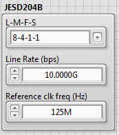
- Select the required L-M-F-S, Line Rate (bps) and Reference Clk Freq (Hz) of JESD204B (JESD link parameters, Lane mapping, byte ordering etc. will be obtained from the INI file).
- Run the Loopback (Host).vi to generate and acquire the required amount of data. The vi will run until the configured size is captured or till timeout.
Note: When PXIe-6591R card is looped using Mini-SAS Loopback adapter at Port0 or Port1, append “-Port0 to Port0” (or) “-Port1 to Port1” to L-M-F-S mode depending on the connection made (say “4-2-2-2-Port0 to Port0”).
Application & Source Download
- Mark as Read
- Mark as New
- Bookmark
- Permalink
- Report to a Moderator
I would like to adapt the RX sample project to receive data from a different device. To which Signal on the DDC connector is the JESD204B SYNC Signal routed?
In the documentation for the RX sample Project testing with ADC12J4000, a "NI MiniSAS to FMC interposer board" is mentioned`, but I could not find documention or a source to order this board.
Is there an overview of the required modifications to adapt the code to a different frame / line rate and a different frame format (e.g. 5 octets / frame)?
- Mark as Read
- Mark as New
- Bookmark
- Permalink
- Report to a Moderator
To which Signal on the DDC connector is the JESD204B SYNC Signal routed?
If you take a look at the top level vhd in the JESD CLIP you'll find the info you're looking for. If you extract the zip you can find it at the following location,
NI PXIe-6591R JESD Sample Project\JESD Sample Project\JESD204B Simple Streaming\CLIP\JESD204B_NI_6591R.vhd. Once you open it up you'll find the following info on line 2363.
    -- Rx SYNC out signal
    DDC_GPIO_Out(0)             <= rx_sync_from_core_r;
    DDC_GPIO_OutEnable_n(0)     <= '0';
In the documentation for the RX sample Project testing with ADC12J4000, a "NI MiniSAS to FMC interposer board" is mentioned`, but I could not find documention or a source to order this board.
My apologies, but mention of the interposer was supposed to be removed from the documentation since it isn't publicly available. I'll look into having the example updated to reflect that.
Is there an overview of the required modifications to adapt the code to a different frame / line rate and a different frame format (e.g. 5 octets / frame)?
If you open the simple streaming example the host vi should have some controls that allow you to modify the line rate and LMFS. Setting up the 6591 in a loopback configuration would be a good place to start when investigating these settings.


