- Document History
- Subscribe to RSS Feed
- Mark as New
- Mark as Read
- Bookmark
- Subscribe
- Printer Friendly Page
- Report to a Moderator
- Subscribe to RSS Feed
- Mark as New
- Mark as Read
- Bookmark
- Subscribe
- Printer Friendly Page
- Report to a Moderator
digsys-05: Rapid Development of Device Interfaces with a Transparent FPGA
Introduction
FPGA development boards feature an FPGA connected to a variety of interesting peripheral devices such as switches, LEDs, RS-232 serial communication, seven-segment displays, and so on. Experimenting with a peripheral’s actual I/O behavior supplements knowledge picked up by reading the data sheet, and provides a sound basis for the design of an FPGA interface to the device.
Developing and debugging a peripheral interface on the FPGA target requires much time, however. Each modification of the VI necessitates a complete rebuild of the FPGA bitstream file, no matter how minor the change. Even for very small designs, waiting two or three minutes to try the modified VI quickly becomes tiresome. Fortunately, the core functionality of many VIs intended for the FPGA target runs quite well on the desktop. Placing the FPGA target in “transparent mode” effectively connects the desktop VI directly to the peripheral device of interest, and iterating the design on the host eliminates the need to rebuild the FPGA target. This article explains how to develop a peripheral interface with a transparent FPGA, and illustrates the technique with an example design process of a two-digit seven-segment display driver for the NI Digital Electronics FPGA board.
Transparent FPGA Concept
LabVIEW FPGA provides ongoing communication between supported FPGA development boards and the desktop computer via the USB cable, even after the bitstream file has been downloaded to the FPGA. The front panel of an FPGA-targeted VI remains visible on the desktop; indicators and controls may be included as on a desktop-targeted VI (or host VI) to display internal FPGA signals and to permit the FPGA behavior to be controlled from the desktop. With only a small amount of additional effort, a pair of VIs – one operating on the host, and another operating on the FPGA – can also communicate through the USB cable. This is the basis for the “transparent FPGA” concept diagrammed below:
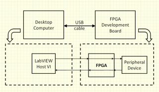
The FPGA VI design is very simple: an FPGA I/O node set to “write” mode (an output signal to the peripheral) is driven by a front-panel control, and a “read” mode FPGA I/O node (an input signal from the peripheral) drives a front-panel indicator. The bitstream file for the FPGA VI need only be created once the first time it is run. Subsequent runs load the bitstream file immediately, provided that no changes have been made.
The host VI design is likewise simple, and requires three subVIs from the FPGA palette. The "Open FPGA Reference" subVI loads the bitstream file to the FPGA and establishes connection to its front panel. The "Read/Write Control" node connects to the FPGA front panel. As part of the host VI shutdown process, the "Close FPGA VI Reference" subVI closes the connection to the FPGA and frees up the reference.
Transparent FPGA VI for Two-Digit LED Display
The two-digit seven-segment LED display on the NI Digital Electronics FPGA board serves as the example peripheral in this article. The complete LabVIEW project is linked at the bottom of this document. If you wish to follow along, be sure to open the LabVIEW project first, and then open the VIs from within the project.
The following video briefly overviews the transparent FPGA VI called "FPGA Pass-Through for Display and Pushbutton", demonstrates its operation on the FPGA board, and details its block diagram construction details:
Even without reading the documentation it is now evident through experimentation that the LED segments are active high and the two digit enables are active low.
Host VI Interaction with Transparent FPGA VI
The follow video shows how to create the host VI "Demonstrate 'FPGA Pass-Through'" to operate the individual signal lines of the two-digit display via the transparent FPGA VI, and demonstrates its operation on the FPGA board:
Now development can proceed much more quickly since design iterations on the host VI do not require FPGA target rebuilds.
Host-Based Development of Two-Digit Display Interface
Now that the host VI has direct control over the two-digit display, the development of a two-digit display interface ultimately intended for the FPGA target becomes straightforward. The display interface to be developed here uses the subVI "Manage Two-Digit Display" to operate the individual segments according to the bit pattern contained in a 16-bit unsigned integer global variable. This subVI contains neither input nor output terminals, and is simply placed in its own area on the block diagram. Other subVIs such as "Show Hex on Display" and "Show Segments on Display" provide a variety of convenient ways to structure information for the display. The former displays an 8-bit integer as a hexadecimal value, and the latter offers individual control of the segments with Boolean arrays.
The following video describes the construction of the host-based prototype of the subVI "Manage Two-Digit Display" that will ultimately reside on the FPGA; this prototype uses the transparent FPGA to permit quick modifications:
Now that the two-digit display manager is operational, the construction of the host-based prototype of the subVI "Show Hex on Display" is detailed in the next video. The ease with which the prototype can be modified while still proving the design on the FPGA development board is also demonstrated:
Conversion of Two-Digit Display Interface to FPGA Target
After establishing correct functionality of the host-based device manager subVI and associated formatting subVIs, converting them to the FPGA target requires little effort. The following video shows how each host-based subVI corresponds to its FPGA-based counterpart:
The next video details the construction of the subVI "Manage Two-Digit Display" intended for the FPGA target:
Demonstration of the Two-Digit Display Interface
The FPGA-targeted subVIs have been debugged and are ready for action. Two top-level VIs "Demonstrate ‘Show Hex on Display’" and "Demonstrate ‘Show Segments on Display’" illustrate how to connect the two-digit display to a user application. View the following two videos to see the block diagram details and a demonstration of the complete display interface operating on the FPGA development board:
Conclusion
Developing FPGA-based interfaces for development devices is a laborious process when a bitstream file must be rebuilt each time the VI is modified. Placing the FPGA in transparent mode permits all development of core functionality to take place on the desktop computer. Structuring the VIs according to requirements of FPGA-targeted allows the host-based VIs to be painlessly converted into their FPGA counterparts.
