From Friday, April 19th (11:00 PM CDT) through Saturday, April 20th (2:00 PM CDT), 2024, ni.com will undergo system upgrades that may result in temporary service interruption.
We appreciate your patience as we improve our online experience.
From Friday, April 19th (11:00 PM CDT) through Saturday, April 20th (2:00 PM CDT), 2024, ni.com will undergo system upgrades that may result in temporary service interruption.
We appreciate your patience as we improve our online experience.
11-11-2017 08:39 AM - edited 11-11-2017 08:57 AM
Hello,
i'm using myRio to read data from K-LC1a radar frontend, which have ramp signal input from -0,5-2 V (based on voltage, it makes chirp sine wave) and mixed signal IF output. The main task is to measure distance.
What i need to do:
Since i have 100kHz wave to sample i need sampling rate on 200kHz+ level, so i see no other option than using FPGA interface.
I calculated that i need 2,5kHz ramp wave at frontend input.
I created "FIFO read" which is running, but i see no other options than int data (analog input and analog output are uword 16bit data).
1. The question is:
Here is my main VI.
2. Can i run simultaneously double FIFO? FIFO Write is "Host To Target" and FIFO Read is "Target To Host ", both DMA. I'm getting error just after Open FPGA reference block. They're compiled. Earlier i did run FIFO Read with no problem.
Here is front panel of VI above and error shown:
Here is my project window:
3. Here is FIFO Read. I defined loop count as 5 us (this stands to 200kHz), but FIFO Read Timeout is tick count. Which clock tick's is it using (internal 25ns or this here 5us)?
4. Here's the same as above, 400us to 2,5kHz. Tried to recalcuted ticks to time, but compile end up with error. Next question is, how should i transfer my elements(matrix) to analog output(element). Here's my doubt.
Greetings,
Solved! Go to Solution.
11-13-2017 08:39 AM
I'm sorry, but can't see edit option. I solved following questions, atm i dont have any.
11-30-2017 10:57 AM
Hello,
I am interested in how you solve.it.Can u tell me in details?
THX very much~My e-mail is 1549829765
11-30-2017 11:02 AM
Hello,
I am interested in the ways that you solve your problems. And I want learn from it. Can you teach me and tell me in details?
Thanks very much!
My e-mail is 1549029765@qq.com
Thanks again~😊
11-30-2017 12:36 PM
Hello Dana_Yang,
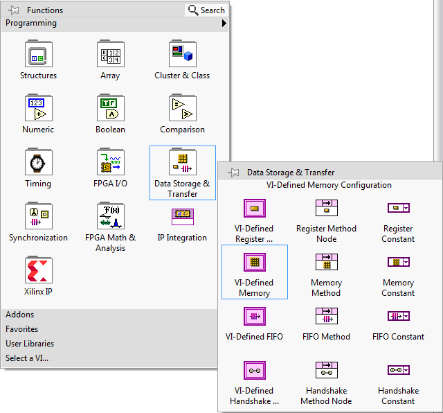
1st of all, You need to create double FIFO method in one FPGA VI. But there's a better way to do it, since if You'll create FIFO to write data, You'll get a delay to communicate host and target that may decrease performance of myRio. Using memory method u can define signal inside of FPGA, and later u can configure it at start of program.
2nd rates, myRio hava a capability to read 500kS/s and write 345kS/s, that gives a clock counter 2us and ~3us.
3rd every input and output of myRio have different voltage range, see documentation (http://www.ni.com/pdf/manuals/376047c.pdf page 10), so if u want to create voltage at specific value, u need to transform it to integer and then transfer it to FPGA module.
4th In method shown up u can run simultaneously reading and writing.
5th Timeout counts as clock cycles (40MHz)
Feel free to ask more questions
Greetings
11-30-2017 09:49 PM
![]() Thank you so much, Szyszku~I am a greenhand in myRIO and desired to learn more about it. Despite I can not comprehense your explain entirely,I feel so excited to get to know "Memory".
Thank you so much, Szyszku~I am a greenhand in myRIO and desired to learn more about it. Despite I can not comprehense your explain entirely,I feel so excited to get to know "Memory".
I don not understand how to use memory, wonder how to transform voltage to FPGA. I will learn more to fix them. It will be wonderful if u teach me more.
THX,😊
12-01-2017 08:22 AM


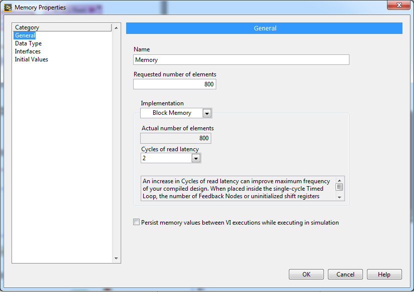
Screen's show how to define memory. How to use it u can see on screens on my earlier post in FPGA. Now how to use them in program and how to convert those numbers to voltage.
1st voltage
As we can see in manual:
First u need to specify what range of voltage You need. I chose analog output C1, cause i need negative voltage -0,5V to 2V. We can read that is MSP connector +/- 10V. So maximum number (9.995V) will be 2047, and maximum negative (10V) will be -2048. Of course resolution is 4.883mV (see manual). Now specify ramp signal or sine to generate voltage that You want (remember to put integer I16(−32,768;32,767) at AO/C1).
U can connect AO with AI to see results or use oscilloscope. Diagram shown post earlier is complete to use FPGA.
Initializing FPGA with defined memory like this will generate ramp signal from 0 to 800*4,883mV=3906,4mV with period of 800*delay defined in Write section (see earlier post). You want to follow like this
Following product should work.
Greetings
12-03-2017 05:46 AM
Thanks a million, Szyszku~
I have some problems, when I use myRIO FPGA.
Can u have a look for me? The link is:https://forums.ni.com/t5/Academic-Hardware-Products-ELVIS/Error-code-61206-to-control-step-motor/td-...
Thx Thx Thx~