- Subscribe to RSS Feed
- Mark Topic as New
- Mark Topic as Read
- Float this Topic for Current User
- Bookmark
- Subscribe
- Mute
- Printer Friendly Page
- « Previous
-
- 1
- 2
- Next »
Zynq 7000 performance
08-21-2013 08:47 AM
- Mark as New
- Bookmark
- Subscribe
- Mute
- Subscribe to RSS Feed
- Permalink
- Report to a Moderator
I'm also involved with the latency issue for control applications and found to my surprise that transfer over the fpga front panel is actually faster (with minimal control/indicators used)!
see http://forums.ni.com/t5/LabVIEW/fpga-host-data-transfer-latency-performance/td-p/2531684
08-21-2013 10:02 AM
- Mark as New
- Bookmark
- Subscribe
- Mute
- Subscribe to RSS Feed
- Permalink
- Report to a Moderator
Hmm, that's interesting. I've always steered clear of controls and indicators because they're supposed to be inefficient but in this case, perhaps the better latency makes them worth a second consideration.
Shane.
08-21-2013 10:23 AM
- Mark as New
- Bookmark
- Subscribe
- Mute
- Subscribe to RSS Feed
- Permalink
- Report to a Moderator
Yes, this is the primary advantage that controls/indicators have for data transfer. If you do the handshaking with IRQs you can avoid having to poll an indicator in order to synchronize. Of course there is a breaking point dependent on how much data you are transferring where the reduced control/indicator latency stops being beneficial. I'm not sure if you'll hit this point in the application you described - you would need to benchmark it.
One caveat I would add here is that if you want to transfer data using controls and indicators, it is best to bit-pack the data and also avoid using arrays. Arrays add inefficiencies for data transfer.
08-21-2013 10:05 PM
- Mark as New
- Bookmark
- Subscribe
- Mute
- Subscribe to RSS Feed
- Permalink
- Report to a Moderator
I actually made a very comprehensive benchmark for latency on RT&FPGA for all modes of transfer and handshaking as well as RT&DAQ a few years ago. I'll post it and my results tomorrow
08-22-2013 01:57 AM
- Mark as New
- Bookmark
- Subscribe
- Mute
- Subscribe to RSS Feed
- Permalink
- Report to a Moderator
Hi Colden
What I am wondering about using IRQs for handshaking: Can I be sure that my new fornt panel value has arrived when the interrupt occures. Intuitively I would suspect that: I write my value to the fpga front panel control, then send the IRQ, which is fast and causes the interrupt on my host, but the front panel value would still be stuck somewhere in the bus overhead...
08-22-2013 10:16 AM
- Mark as New
- Bookmark
- Subscribe
- Mute
- Subscribe to RSS Feed
- Permalink
- Report to a Moderator
Hello Tom,
You don't need to worry about a synchronization error there - the FPGA interface functions that read I/O from the FPGA will block until the data arrives. The purpose of the IRQ is just to ensure that the RT side waits until after the FPGA has updated the value before reading it. When the host side system calls the I/O read function it waits for the data to arrive from the FPGA.
You can look at the IRQ examples in the example finder for more information as well.
08-22-2013 10:22 AM
- Mark as New
- Bookmark
- Subscribe
- Mute
- Subscribe to RSS Feed
- Permalink
- Report to a Moderator
OK I made these benchmarks and the attached code December 3rd 2010... so they are a little out of date. I think I used a PXI-8108 or 8110 and a PXI R series card. Although you could run the attached code on any target (Including the 9068) and get latency numbers today. I've also noticed, since then, that our PXIe controllers have higher latency when interacting with PXI R series cards... I'm guessing that is because the PCIe-PCI bridge.
Here is my write up from 2010:
I'm doing some testing for how fast I can possibly do this sequence:
- Real life event (rising edge on digital pin)
- RT detects this
- Read from an RT FIFO
- Read from analog inputs
- Execute a subVI (nearly empty placeholder in this case, inlined). Could be a model
- Write to analog outputs
- Write to an RT FIFO
Basically the hardware timed single point (HWTSP) use case... except the analog outputs are software timed as I want to push those out ASAP... not wait for the next tic.
I used an oscilloscope to measure the time between the rising edge and the AO to get the latency numbers. For FPGA I was also able to timestamp the turnaround time in FPGA so I didn't need a scope, but the scope confirmed the #s I got from the FPGA.
I tried four hardware configurations:
- R Series to C series IO (9401 & 2x9215 & 9263)
- R Series built in IO (7854)
- PXI-6289 (M Series MIO)
- PXIe-6368 (X Series SMIO)
In the FPGA configurations, I did 8 AI and 4 AO. I did four FPGA software configurations:
- DMA. The RT code blocked on a DMA causing 100% CPU usage until the FPGA acquires the data. RT then gets the data, reads an RT FIFO, calls my subVI writes an RT FIFO and writes a DMA back down to the FPGA.
- DMA + IRQ. Same thing as DMA but instead of blocking on the DMA at 100% CPU usage I block on an IRQ. Theoretically this should increase latency and jitter but save CPU.
- Registers. RT code hard polls a boolean FPGA register (indicator) causing 100% CPU usage until the FPGA acquires data and sets that register to true. RT code then reads the registers (indicators) for the AI data, reads an RT FIFO, calls my subVI, writes an RT FIFO and writes registers (controls) back to the FPGA... including one boolean 'go' register to true. The FPGA during that time was hard polling the 'go' register... and when it is true... reads the AO register controls and pushes them to analog outputs.
- Registers + IRQ. Same thing as registers but instead of hard polling use an IRQ. Theoretically this should increase latency and jitter but save CPU.
All times in uS.
| Test | 7813R to C Series IO | 7854R Built in IO |
|---|---|---|
| DMA | 41 | 23 |
| DMA & IRQ | 57.5 | 39 |
| Registers | 31.5 | 12 |
| Registers & IRQ | 46 | 26 |
As expected registers was the fastest.. and ADC conversion time (1/sampling rate) plays a huge role in I/O turnaround latency.
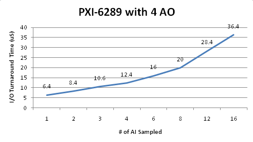
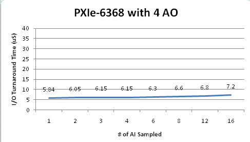
In the DAQ configurations I tried a variety of AI and 4 AO, as it is easy to rapidly change my # of AI. I made a graph of the DAQ timing. A timed sequence was used with a while loop inside so I could do processor assignment and avoid interrupts. The code blocked on the DAQmx Read which was set to polling mode through a DAQ property node. This gave significantly better numbers than using a timed loop with a DAQ timing source string (interrupt mode). I don''t even include the timed loop (interrupt mode) numbers here since they were so much worse. For the MIO card, I set the AI.ConvertClock to its maximum (500,000) so the multiplexing was as fast as possible.
It appears that the major slowdown is the D/A and A/D update rates and multiplexing. The D/A and A/D update rate of the DAQ cards and built in IO of the 7854 are much faster than the C series expansion (100kS/s/ch). Also, as I add AO, the times hardly change at all because there is one D/A per channel. As I add AI, the time doesn't change much unless you have a multiplexed AI device.
Also, I've benchmarked the time using the input and output RT FIFOs as only 0.6uS.... and that time is included in these results. It was only an 8 element FIFO though.
The code is attached. There are three top level VIs, one for DAQ interrupt, one for DAQ polling, and one for FPGA (all modes).
I then increased my stimulus rate (pulse train) to try to achieve the highest loop rate possible. Theoretically I should be able to hit the inverse of the latency in frequency. The configuration I tried was the PXI-6289 with 2 AI and 4 AO, which is 8.4uS, so I should hit around 119 kHz. Somehow I was actually able to loop dead stable at 160 kHz. At 161 kHz, DAQ reported being late. At this time, I don't know why I was able to loop faster than my latency. If I looked at the oscilloscope, I saw my AO updates were after the next rising edge.
Big takeaways for high-end performance:
- Use polling instead of interrupt
- Can half your latency times, enabling higher loop rates
- If you use interrupt mode, you save CPU on the core your DAQ/FPGA code has been assigned to... but you give up CPU on core 0 as RT has to service the interrupts. So you end up with no real CPU gain.. and considering you're latency times are higher and your loop rate is slower... you end up with a net loss.
- Use the RT SMP VIs to 'reserve' the core that will be doing your HWTSP
- Use the fastest D/As and A/Ds you can get... these a major contributors to the latency times and therefore loop rate.
- Don't have any shared resources between loops assigned to different cores
- I accidentally had a functional global shared between my two timed loops, it dropped my loop rate from 160kHz to 11kHz.
- Reading/writing RT FIFOs doesn't significantly contribute to latency/loop rate... at least for my 8 element ones.
01-15-2014 05:16 AM - edited 01-15-2014 05:22 AM
- Mark as New
- Bookmark
- Subscribe
- Mute
- Subscribe to RSS Feed
- Permalink
- Report to a Moderator
Hmm, I finally got around to reading that last post and trying to understand it.
The benchmarks presented don't really reflect what we're trying to do.
In our system, the FPGA DMA FIFOs rule the world. We clock our FPGA card with an external clock (10MHz nominally) so we have an inherantly unsynchronised FPGA and RT system. We read 56 U32 elements at a time. We write 16 U32 elements at a time. The FPGA control loop runs at 1MHz frequency and the rate at which the FPGA sends data (oversampled accordingly) to the RT system is configurable. Thus we can have any multiple of 1us data transfer frequency (at 56 U32 elements each) between FPGA and RT.
This variable frequency communications between FPGA and RT combined with the non synchronous nature of the FPGA and RT clocks requires us to do some "magic" with the timing settings for the timed loop on the RT system. We monitor the time taken to read the DMA FIFO (from FPGA), whether the FIFO has data remaining after the read (Fixed length reads) and whether the last loop finished late or not (Timed loop). We then adjust the period value for the timed loop in order to keep the DMA reads and Timed loop as closely synchronised as possible (We need the CPU cycles to take care of TCP traffic and other matters). We run our RT system as a single-core machine with Hyper Threading disabled.
So our loop comprises of:
1. Read DMA FIFO from FPGA
2. Do some processing
3. Write DMA FIFO to FPGA
We also use some RT FIFOs, but the latency of these is as correctly noted here is acceptable.
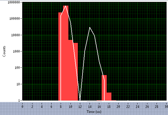
What we see is that when we monitor the time taken to read from a DMA channel from the FPGA, the distribution of our timings looks very much like the polling rate of the DMA buffer inttroduces a timing quantisation of 6 us. Below is a histogram of our timings for reading (White line) and writing (red columns) the DMA FIFOs from and to the FPGA respectively. It's a distribution which can actually play havok with out control loop. Our entire loop rate needs to be 50us (20kHz rate) and taking a 6 us hit every now and then depending on how the DMA FIFO is behaving seems like a lot. I have seen this 6us timing previously when I was benchmarking the DMA channels completely independently of our control software.
We timed this using a us Timer before and after the FIFO read. Any variations in the execution time of this node will of course also be reflected here. Our hardware is a PXIe-8115 with a PXIe-7965R FPGA card.
Even in cases where we are running behind in our timings (where the FIFO from the FPGA has plenty of data for reading) we never see the FIFO read executing any faster than 8 or 9 microseconds (let's say 8.5 us).
I had high hopes installing the "new" Patch which should apparently reduce jitter but it seems to have had absolutely no affect on our software whatsoever.
It is with this background that I was extremely interested in any changes in the execution speed of DMA FIFOs with the new Zynq architecture.
Shane.
PS I will state again that once you increase the amount of data being transferred so that the ACTUAL data transfer takes longer than the 6us mentioned here, each U32 sample sent adds 0.06us to the execution time of the DMA. Tht's 1/100th of the minimum required time for a DMA read or write.
02-04-2014 04:55 AM - edited 02-04-2014 04:57 AM
- Mark as New
- Bookmark
- Subscribe
- Mute
- Subscribe to RSS Feed
- Permalink
- Report to a Moderator
So I have a small benchmark VI which pretty much demonstrates what I'm getting at. This is becoming a bit current because we're starting to look at the architecture for our next software version and the latency of the DMA transfers is biting us a little bit to be honest. We MAY end up with a mixed approach of FP controls and DMA in order to reach our goals. Nothing is certain yet.
But back to the benchmark.
I have tried to benchmark the DMA performance when shifting 32MB of data across DMA FIFOs of varying width. I have implemented U8, U16, U32, U64, FXP8, FXP16, FXP32, FXP64 FIFos each with its own return queue so that I cen accurately benchmark the time taken for all the data to arrive on the FPGA. I create an array of 32MB size (32M U8 or FXP8*, 16M U16 or FXP16*, 8M U32 or FXP32* and 4M U64 or FXP64*) to transfer and then send the data via DMA FIFO and wait for a response from the FPGA that all have arrived. Subsequent runs then split this payload up into successively smaller packets and measure the overall time taken to deliver the content. The inherent overhead of the DMA transfer thus increases rapidly as we decrease the packet size. Note that the total amount of data* transmitted is constant for all cases.
This test was run on a PXIe-8115 with a PXIe-7965R FPGA card.
*Caveat: I know FXP is represented as 64-bit on the RT level meaning that an array of 32M FXP8 is actually 8x32MB in size but the actual DATA CONTENT is 32MB. I still believe that the sriver should automatically choose the next largest FIFO size for transfer. But this is just for the case where this may be changed in a future version. The scaling seen between the FXP tests is solely due to the fact that internally the FIFOs are working with 64-bit width meaning that the FXP8 version is actually sending 8x more data over the DMA FIFO than the FXP64 version.
So we see for example that sending the data in packets of 4 instead of packets of 4M is overall 100 times slower for U8 and nearly 200 times slower for U16, U32 and U64. An ideal (not achievable) scenario with zero overhead would yield the same times for all packet sizes. What I would be interested in is seeing how the times vary with packet size for the newer Zynq systems. Given the very low latency bus over which the DMAs are being transmitted, it should be feasible for the increase in overall time with decreasing packet size to be lower than we see here.
Once we get to packet sizes of below 100 the times tend to even out. This agrees with previous tests I have made where sending 1 element or sending 100 elements or anything in between will take the exact same amount of time. Thus, moving to smaller packets we are simply seeing a linear increase of the overhead of the individual DMA write calls instead of the data size itself being the performance determining aspect.
I include the VIs here in case someone might want to try this code out on the newer targets. If the DMA transfers on the newer targets using the AXI bus for transmission could significantly lower the overhead for writing single elements to the DMA then this allows a very different approach for control applications which require small amounts of data to be exchanged as quickly as possible (like ours).
Shane
02-07-2014 02:23 AM
- Mark as New
- Bookmark
- Subscribe
- Mute
- Subscribe to RSS Feed
- Permalink
- Report to a Moderator
- « Previous
-
- 1
- 2
- Next »


