From Friday, April 19th (11:00 PM CDT) through Saturday, April 20th (2:00 PM CDT), 2024, ni.com will undergo system upgrades that may result in temporary service interruption.
We appreciate your patience as we improve our online experience.
From Friday, April 19th (11:00 PM CDT) through Saturday, April 20th (2:00 PM CDT), 2024, ni.com will undergo system upgrades that may result in temporary service interruption.
We appreciate your patience as we improve our online experience.
09-13-2015 10:07 PM
Hi All,
I'm trying to setup a simple VI on a myRIO-1900 to use a digital potentiometer as a variable resistor. I have preciously used an SPI dpot with success however I am having issues when switching to an i2C controlled dpot.
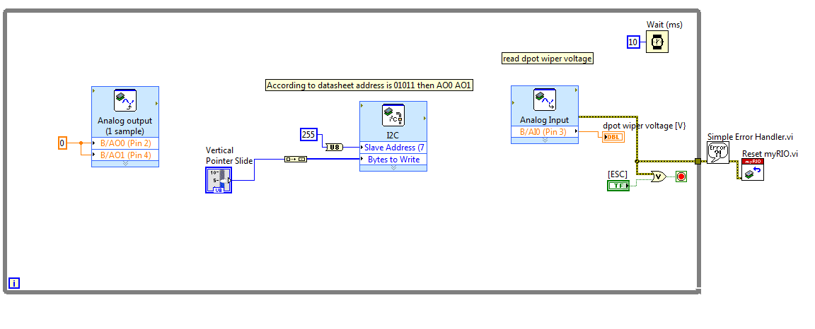
Following the datasheet found here ( http://www.analog.com/media/en/technical-documentation/data-sheets/AD5241_5242.pdf ) I have made the following connections.

Solved! Go to Solution.
09-14-2015 04:23 PM
From page 5 of your manual, it looks like the communications is accepted in the format of slave address, instruction byte, data byte. From what I'm seeing of your code, it appears that you are missing the instruction byte. The input to "Bytes to Write" should be in the format of a 1D array, so you should be able to feed a 2-element array in with the instruction byte as the first element and the data as the second.
In addition, it looks like your address might be wrong. It should be 01011000 (the last digit is 0 because write enables at low; page 5 of manual), which should be 88 and not 255 as you have it.
This is what I can see so far. Hopefully this helps!
09-16-2015 12:15 AM
You might be onto something with regards to the instruction byte. According to the datasheet I'm assuming I do not ned to select an RDAC as I am using the AD5241 with one potentiometer, I have no need for a midscale reset and SD is active high so I would want this to be low therefore for the instruction byte I can send a 00000000 byte then use the build array function to subsequently add the 8 bit data for the "data byte"? Or should I be using a different method of sending these two elements?
09-17-2015 10:35 AM
My assumption was a 1D array of two elements, the first being the instruction byte and the second being the data byte. However, that's just my educated guess; if you're looking for more information, I might ask the makers of the AD5242 for more information.
09-20-2015 09:10 PM
Thankyou TheXiadow, a 1D array of two elements was the solution. Also, I had damaged two of my chips through overheating so a new chip + correct instruction and data bytes was teh trick.
09-21-2015 12:25 PM
Great! Glad we were able to figure that out.
Cheers!
12-16-2015 04:30 AM
Hi,
I am having problem in I2C communication with AD5241. The slave device address is 0x58 (for write) and 0x59 (for read).
The problem i am facing is when i am sending the slave address, the device is sending ACK but when i send the instruction byte(0x00) the device is sending NACK.
I am able to read the RDAC value in read mode. But i am unable to write any value to RDAC. What might be the instruction byte should i send.? Please help me with the issue. Thanks.
12-17-2015 03:37 PM
What instruction byte are you sending? Specifically, I might suggest looking into what values you have set for the output logic pin values, and if what you are setting them as is what you expect. There's a little more information on those two pins on page 3.
12-17-2015 03:38 PM
It also looks like you're posting on an older post that has been resolved -- more people might see it if you start a new post!
12-17-2015 10:21 PM
the instruction byte that i am sending is 0x00 and sometimes 0x40 if i want midscale reset. The Output logic pins are grounded and voltage levels are as expected only..