- Subscribe to RSS Feed
- Mark Topic as New
- Mark Topic as Read
- Float this Topic for Current User
- Bookmark
- Subscribe
- Mute
- Printer Friendly Page
Trace to Pads Net Group Options not Avalible
02-10-2010 07:44 AM
- Mark as New
- Bookmark
- Subscribe
- Mute
- Subscribe to RSS Feed
- Permalink
- Report to a Moderator
Hello, To explain my problem I have prepared as easy example as it is possible.
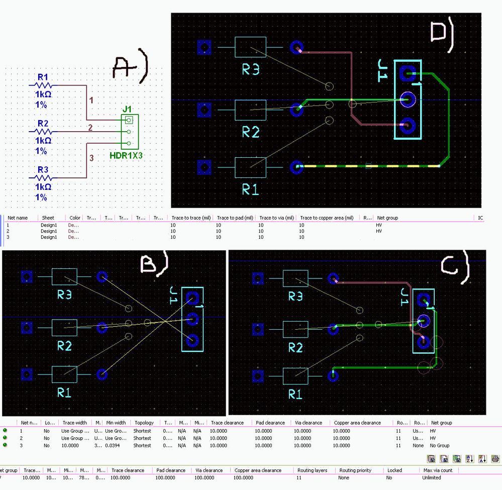
Let suppose that we have a circuit diagram that is shown below in the attached figure (Figure A). As can be seen the circuit diagram consists of three resistors R1, R2, R3 and one connector J1. These parts are connected each other by three nets 1,2 and 3. Nets 1 and 2 is grouped into HV group with a Multisim clearance option (to trace, to pads, to copper parts) equal to 10 mil. In Ultiboard this HV group in Net Group Tab is set to clearance option (to trace, to pads, to copper parts) equal to 100. It results from the fact that both lines (1,2) exhibit, in example 1000V, while net 3 only 10V. Thus these nets, namely 1 and 2 posses internal clearance 10 mil to each other and external 100 mil with respect to the net 3. Up to now everything works fine but when we turn on the Autorouting option for a given geometry configuration (Figure B) it will produce complete disaster (Figure C). As can be seen in figure C), the Autorouter does not take into account the “Group HV” clearance to the pads. The green trace from Resistor R1 to connector J1 should look more likely like in Figure D.
My question is: Why the Ultiboard does not take into account the Group HV clearance to the pads. ??????
I was trying to solve this problem in many different ways.
In example, I have changed manually the pad clearance of a connector J1 to a given value. It works – the Autorouter will produce the result that looks like in figure D), but it will produce the clearance to each net independently of a net group that it belongs !!!!!.
In the J1 part pad clearance option one can set “Use net settings” – but it will produce only 10 mil clearance for pads. Why there are no option “Use Net Group settings” ????????? I mean that a clearance of a pad is different for different groups or nets !!!!!!!

02-12-2010 04:26 AM
- Mark as New
- Bookmark
- Subscribe
- Mute
- Subscribe to RSS Feed
- Permalink
- Report to a Moderator
I was thinking about this problem a lot and unfortunately I have found much more important problems that only this presented above !!!!!.
If someone look more precisely into Attached (above) figure C, one can immediately see that even the CRC check and Design Rule Check does not work properly in Multisim 11 !!!!!!!.
Namely. the low voltage red trace (net 3), that is of course wrong autorouted - goes to close to high voltage green nets 1 and 2 (close to connector j1), is not underlined by red circle by Design Rule Check. In contradiction the bottom green trace (net 1) is underlined by Design Rule Check since it goes too close to pad of a connector J1 connected to net 3.
If some one suppose that autorouter does not work properly the Design Rule Check should does !!!!!!. This bug should have to be fixed ASAP (as soon as possible) or it may causes a lot of troubles !!!!
By the way, I am thinking that main idea of software is not well designed. From my point of view, in principle, THT/SMD pads and vias should do not have own clearance option if they are connected to the net. If they are connected, they should automatically exhibits net clearance properties - that is physically clear.
I have found a lot of mismathes with this software but at the moment I hope that someone could help me with this problem at first 🙂
Best Regards
Irocz02-13-2010 06:58 AM
- Mark as New
- Bookmark
- Subscribe
- Mute
- Subscribe to RSS Feed
- Permalink
- Report to a Moderator
Hello, it’s me once again.
I am really disappointed that there are no any answers.
But I am still finding bugs, one by one 😞
In example the tool “Follow me” does not work properly with this example as well.
If someone would try to connect this manually via “Follow-me” tool, one would immediately see that during operation the clearance of a given net is not taken into account. The connection tool takes only the clearance of a net that we are approaching during manual routing. But this is not true if the net that we are using exhibits higher clearance properties :(.
We will be lucky if the DRC check underline this mismatch in clearance properties, but sometime it doesn’t !!!!!! as shown above.
02-17-2010 06:08 AM
- Mark as New
- Bookmark
- Subscribe
- Mute
- Subscribe to RSS Feed
- Permalink
- Report to a Moderator
Hello, it’s me once again.
I have already made a lot of tests with different examples and I have the following ideas, solutions and propositions:
1) The main algorithm “engine” of the software does not work properly, namely during the operation the algorithm does not take into account the clearance properties of a net that is currently under construction. The engine takes only the clearance properties of a nets/vias/pads which are approached during the engine operation. This result in substantial amount of mistakes in “Follow-me”-tool and Autorouter.
Possible solutions: Actually, there are no easy solutions - I am working on it and I am trying to elaborate procedure that may helps.
2) The main idea of software is also not perfect. In principle, THT/SMD pads and vias should do not exhibit own clearance properties if they are already connected via nets. If a net exhibit 1500 Volts (clearance = 200 mil) then the THT-pad should at lest exhibits the same clearance property. In Ultiboard it is set to 10 mils for each pad. This may results in substantial amount of mistakes in “DRC check rule”
Possible solutions: One can manually change the clearance properties of a pads/vias. But this is not good solution especially if there exists a lot of parts with different pads configurations and different nets connection configuration (It takes a lot of time to carry it out precisely). Moreover it does not help if in our design there are different Net groups. There are not “Use net Group” option thus pad/vias exhibit the same clearance property for ever and with respect to all others nets independently of the group that they belongs.
Above mentioned problems are crucial in high voltage electronics (staring from 115V). Thus NI Design suite is not suitable for this type constructions (power supplies). It works properly with certain conditions, i.e. with low voltages.
02-17-2010 09:57 AM
- Mark as New
- Bookmark
- Subscribe
- Mute
- Subscribe to RSS Feed
- Permalink
- Report to a Moderator
Hi,
I see that you use Multisim very intensivly and you are asking hard questions!
Although National Instruments practice is that answers to the posts give local support engineers, in this case we have forwarded your question directly to Multisim support engineers which have better knowledge and deeper understanding about Multisim!
Although they maybe also do not have solution to your problem, I hope they will offer there view of the problem soon!
Best regards
Franjo Tonkovic
National Instruments
Applications Engineer
02-18-2010 12:54 PM
- Mark as New
- Bookmark
- Subscribe
- Mute
- Subscribe to RSS Feed
- Permalink
- Report to a Moderator
Hi Irocz,
I've created a test circuit similar to what you have shown and I can confirm that the Autorouter did violate the clearance settings. But to be honest, with your setting and the component you selected it is not possible not violate the DRC errors. The component J1, I am assuming this part is from the Master database, the center to center distance between the pins is 100 mil so it is not possible for you to route any trace with a 100 mils clearance to these pins without triggering the error.
I prefer to have one clearance setting each of my net, I don't like to have clearance setting to trace, via and pad separately and base on your comments, I think you would agree. You can turn off the separate clearances setting by selecting Options>PCB Properties>>Design Rules, uncheck the "use multiple clearances" box and now your only clearance setting is trace clearance.
In general, if you have nets that you need to control such as the high voltage nets, I would recommend you manually route these using the Place>>Line method, you have full control where the wires goes and once you finished, lock down the traces and then use Ultiroute to route the rest of you PCB.
Best regards,
Tien Pham
National Instruments
02-19-2010 07:38 AM
- Mark as New
- Bookmark
- Subscribe
- Mute
- Subscribe to RSS Feed
- Permalink
- Report to a Moderator
Hi Tien P,
Thank you very much for your response, it is of great importance for me.
I see that you do not understand how big mistakes have you made. To show this once again I have improved above presented example taking into account propositions of Tine P. At first I have uncheck the "use multiple clearances" box and increase the distance between pins of a connector J1. Secondly I have routed manually, as proposed by Tine P, the high voltage nets. Then I have just simply push the autorouter button. The result is presented in the figure attached to this e-mail.
The low voltage green net is of course wrong autorouted. It goes to close to high voltage THTpads that also exhibit high voltage!!!!!!!. But this is piece of cake. The biggest problem is that this problem is not underlined by DRC check rule and this is a complete disaster. In example, if I will produce 100000 of such PCB boards since I ma sure that there are no any DRC problems, who will be responsible for discharge between high voltage net and low voltage one close to the connector J1.
P.S. Unfortunately the proposition of Tien Pham makes the case even worst. Thus I was trying to fix this problem with "use multiple clearances" i.e. for THTpads.
P.S. For better understanding, I have attached the example Ultiboard file to this e-mail. After opening the file just simple push the autorouter button and try to find DRC error.
I am looking forward to hearing from you
Best Regards
Irocz
02-25-2010 01:38 PM - edited 02-25-2010 01:39 PM
- Mark as New
- Bookmark
- Subscribe
- Mute
- Subscribe to RSS Feed
- Permalink
- Report to a Moderator
Hi Irocz,
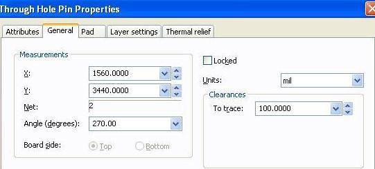
If you don't want net 3 to come too close to pad 1 and 2 on the header, you can set the pad clearance to 100 mils. Double click on the pad and select the "General" tab to change the clearance setting.
Attached is the modified file.
As for the design rule, select View>>clearances to turn on the clearances. I like to use this to help me understand why I am getting DRC errors and in your example, I don't see any reason why Ultiobard should report a DRC error.
Best regards,
Tien Pham
National Instruments

